Multilayer ceramic capacitor and method for manufacturing the same

a multi-layer ceramic and capacitor technology, applied in the direction of fixed capacitors, basic electric elements, electrical appliances, etc., can solve the problems of reducing yield, difficult to manufacture a sintered body composed of fine-grain barium titanate crystal grains, and significant grain growth, so as to improve the relative dielectric constant, temperature characteristic, and temperature characteristic, the effect of suppressing the grain growth of crystal grains

Active Publication Date: 2008-10-07
KYOCERA CORP
View PDF8 Cites 28 Cited by
  • Summary
  • Abstract
  • Description
  • Claims
  • Application Information

AI Technical Summary

Benefits of technology

[0014]The present invention aims at providing a multilayer ceramic capacitor that can suppress the grain growth of crystal grains when a dielectric ceramic composed of barium titanate crystal grain in which part of Ba is substituted by Ca, Sr or part of Ti is substituted by Zr is used as a dielectric layer, and that can improve relative dielectric constant, temperature characteristic, and high-temperature load test characteristic in high-volume manufacturing which uses, for example, a tunnel-type large kiln, as well as a method for manufacturing the same.
[0022]This can reduce variations in grain growth between crystal grains (for example, the BCT crystal gain and the BST crystal grain), and also improve relative dielectric constant, temperature characteristic, and high-temperature load test characteristic. In high-volume manufacturing of a multilayer ceramic capacitor with use of a tunnel-type large kiln that undergoes large variations in maximum temperature during firing, the above-mentioned dielectric layer is stable in the relative dielectric constant, temperature characteristic and high-temperature load test characteristic, thereby increasing the yield.
[0024]This stabilizes the relative dielectric constant and temperature characteristic of a dielectric layer whose main crystal grains are dielectric powders that differ from one another in at least one selected from Sr composition concentration and Zr composition concentration (for example, the BCT crystal grain and the BT crystal grain), when high-volume manufacturing of a multilayer ceramic capacitor is performed by a tunnel-type large kiln that undergoes large variations in maximum temperature during firing. This also stabilizes the high-temperature load test characteristic of a multilayer ceramic capacitor including this dielectric layer, thereby easily increasing the yield.

Problems solved by technology

Especially, the use of raw material whose particle diameter is not more than sub-micron may cause significant grain growth.
It is therefore known that it is not easy to manufacture a sintered body composed of fine-grain barium titanate crystal grains.
Therefore, the grain growth of BCT crystal grain is apt to cause variations during high-volume manufacturing, so that there occurs many poor in relative dielectric constant, temperature characteristic, and high-temperature load test characteristic, thereby lowering the yield.
However, even with such a high dielectric constant material, the same problem as described above is occurring in high-volume manufacturing.

Method used


Image

  • Multilayer ceramic capacitor and method for manufacturing the same
  • Multilayer ceramic capacitor and method for manufacturing the same
  • Multilayer ceramic capacitor and method for manufacturing the same

Examples


first preferred embodiment

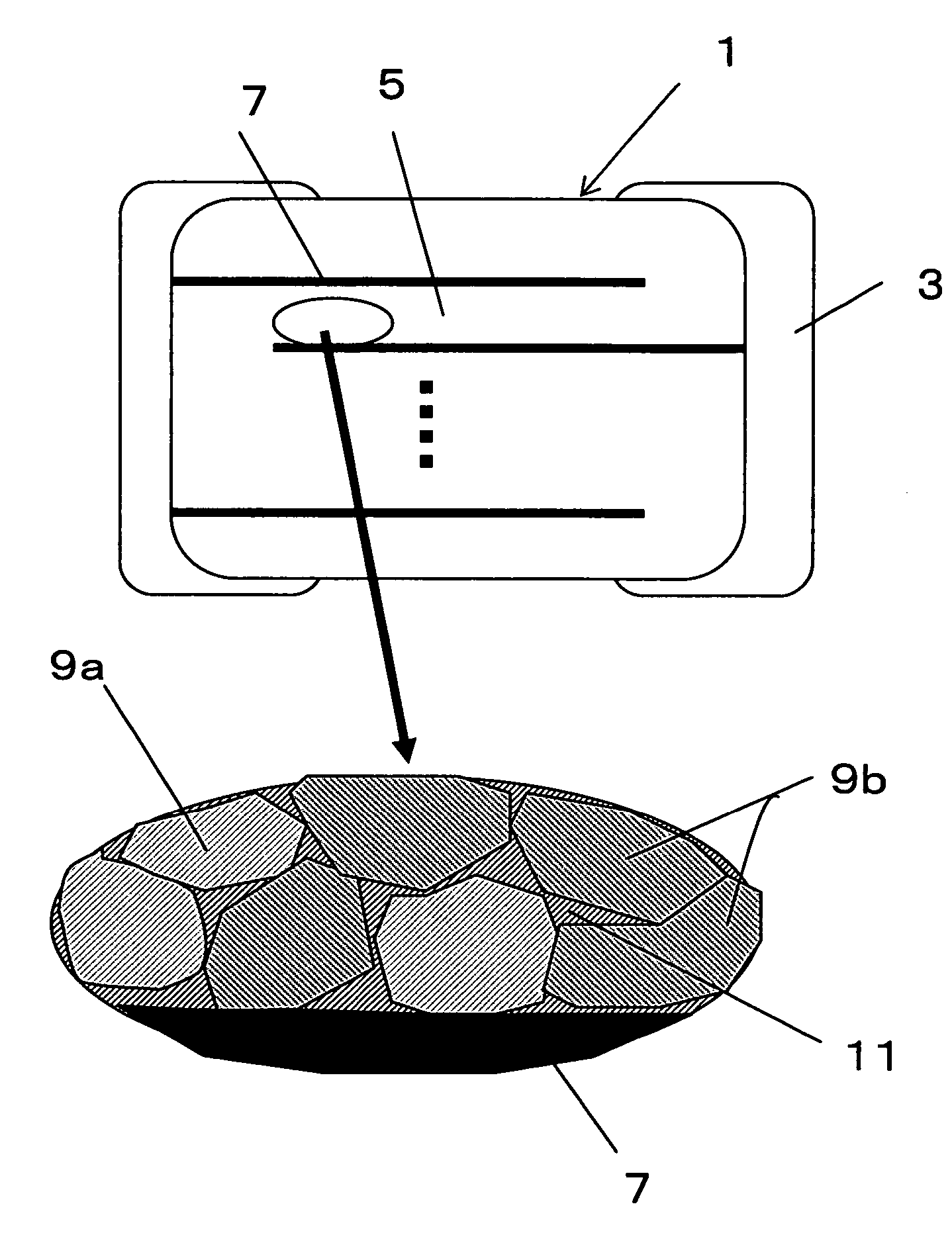
[0030]A multilayer ceramic capacitor of the invention will be described in detail with reference to FIG. 1. FIG. 1 is a schematic sectional view showing a multilayer ceramic capacitor of the invention, and a partially enlarged view in FIG. 1 is a schematic diagram showing a main crystal gain and a grain boundary phase that constitute a dielectric layer. In this multilayer ceramic capacitor, an external electrode 3 is formed at both ends of a capacitor body 1, respectively. The external electrode 3 can be formed, for example by baking Cu or an alloy paste of Cu and Ni.

[0031]The capacitor body 1 is formed by alternately laminating a dielectric layer 5 and an internal electrode layer 7. The dielectric layer 5 is composed of crystal grains 9a, 9b, and a in boundary phase 11. It is preferable for miniaturization of the multilayer ceramic capacitor that the dielectric layer 5 has a thickness of not more than 3 μm, especially not more than 2.5 μm. To stabilize variations in electrostatic c...

second preferred embodiment

[0075]A second preferred embodiment of the invention will next be described. Although the description overlapping with that of the first preferred embodiment has left out of the following, the second preferred embodiment is the same as the first preferred embodiment, except that the foregoing BCT crystal grain is replaced with BST crystal grain (namely, perovskite barium titanate crystal grain in which part of A site is substituted by Sr). Therefore, in the following, reference is made to the same drawing as the first preferred embodiment, particularly FIG. 1 and FIG. 4, and the some reference numeral “9a” has been retained for the BST crystal grain.

[0076]Crystal grains 9a and 9b constituting a dielectric layer 5 of the second preferred embodiment are crystal grains that consist mainly of Ba and Ti, and differ from one another in Sr composition concentration. Specifically, these crystal grains are a perovskite barium titanate crystal grain (BST crystal grain) in which part of A site...

third preferred embodiment

[0088]A third preferred embodiment of the invention will next be described. Although the description overlapping with that of the first preferred embodiment has left out of the following, the third preferred embodiment is the same as the first preferred embodiment, except that the foregoing BCT crystal grain 9a is replaced with a BCTZ crystal grain. Therefore, in the following, reference is made to the same drawing as the first preferred embodiment, and the same reference numeral “9a” has been retained for the BCTZ crystal grain.

[0089]Crystal grains 9a and 9b constituting a dielectric layer 5 are crystal grains that consist mainly of Ba and Ti, and differ from one another in Ca composition concentration and Zr composition concentration, specifically perovskite barium titanate crystal grain (BCTZ crystal grain 9a) in which part of A site is substituted by Ca and part of B site is substituted by Zr, and perovskite barium titanate crystal grain (BT crystal grain 9b) containing neither ...


PUM

PropertyMeasurementUnit
concentrationaaaaaaaaaa
mole ratioaaaaaaaaaa
temperatureaaaaaaaaaa

Abstract

Provided is a multilayer ceramic capacitor having a capacitor body formed by alternately laminating a dielectric layer and an internal electrode layer, and an external electrode formed on both ends of the capacitor body. The dielectric layer has at least two type of barium titanate crystal grains that differ from one another in at least one selected from Ca composition concentration, Sr composition concentration, and Zr composition concentration, and a grain boundary phase. If this multilayer ceramic capacitor employs, as a dielectric layer, a dielectric ceramic that contains barium titanate crystal grains in which part of Ba is substituted by Ca, Sr, or Zr, it is capable of suppressing the grain growth of crystal grains, and improving relative dielectric constant, temperature characteristic, and high-temperature load test characteristic, for example, in high-volume manufacturing using a tunnel type large kiln.

Description

[0001]Priority is claimed to Japanese Patent Applications No. 2004-340347 filed on Nov. 25, 2004, No. 2004-371317 filed on Dec. 22, 2004, No. 2004-373173 filed on Dec. 24, 2004, No. 2004-373180 filed on Dec. 24, 2004, and No. 2004-373181 filed on Dec. 24, 2004, the disclosure of which is incorporated by reference in its entirety.BACKGROUND OF THE INVENTION[0002]1. Field of the Invention[0003]The present invention relates to a multilayer ceramic capacitor and a method for manufacturing the same. Particularly, the invention relates to a small-sized multilayer ceramic capacitor of large capacity and high reliability in which a dielectric layer is composed of barium titanate crystal grains that differ from one another in at least one selected from Ca composition concentration, Sr composition concentration and Zr composition concentration, as well as a method for manufacturing the same.[0004]2. Description of Related Art[0005]In recent years, as mobile equipment such as cellular phones a...

Claims


Application Information

Patent Timeline
Patent Type & Authority Patents(United States)
IPC IPC(8): H01G4/06
CPCC04B35/4682C04B35/49C04B35/62665C04B35/62805C04B35/6281C04B35/62815C04B35/6303C04B35/64H01G4/1218H01G4/1227B32B2311/22C04B2235/3206C04B2235/3208C04B2235/3213C04B2235/3215C04B2235/3224C04B2235/3225C04B2235/3244C04B2235/3262C04B2235/36C04B2235/5445C04B2235/6025C04B2235/656C04B2235/6582C04B2235/6584C04B2235/663C04B2235/72C04B2235/782C04B2235/785C04B2235/79C04B2235/85C04B2237/346C04B2237/405H01G4/06H01G4/30H01G4/00
Inventor IWASAKI, KENICHIFUKUDA, DAISUKENISHIGAKI, MASAHIROMATSUBARA, KIYOSHIKAMIGAKI, KOUSEI
Owner KYOCERA CORP
Why Eureka
Try Eureka