Method of manufacturing a semiconductor heterostructure

a semiconductor heterostructure and manufacturing method technology, applied in the direction of basic electric elements, nanotechnology, electric instruments, etc., can solve the problems of unsuitable surface properties of semiconductor heterostructures, unsuitable for further use, and inability to apply the above described prior art processes, so as to reduce the thermal load of the donor wafer, reduce the surface roughness of the ungraded smoothing layer, and reduce the effect of surface roughness

Active Publication Date: 2008-12-02
SOITEC SA
View PDF13 Cites 20 Cited by
  • Summary
  • Abstract
  • Description
  • Claims
  • Application Information

AI Technical Summary

Benefits of technology

[0014]It is the surprising finding of this invention that a so-called “inverted-bonding” between the donor wafer and the handle wafer can be applied without difficulties by providing the smoothing layer between the graded buffer layer and the top layer, wherein the value of the in-plane lattice parameter of the smoothing layer is chosen such that it is in between the value of the first and second lattice parameter. By means of this arrangement, the surface roughness of the ungraded smoothing layer is reduced compared to the surface roughness of the underlying graded buffer layer. As a consequence, the surface roughness of the donor wafer is reduced in comparison to the state of the art heterostructures and the donor wafer can be bonded directly with the handle wafer without the necessity of depositing an insulator layer on the top layer of the donor wafer before bonding. This is due to the fact that the top layer grows on a strained but smooth surface of the underlying smoothing layer. Due to the omission of a formation of an insulator layer on the donor wafer, the thermal load on this wafer can be reduced and all of the above mentioned disadvantages connected therewith do not apply although the donor wafer can be bonded with the handle wafer especially well.

Problems solved by technology

The structure obtained usually has a surface morphology that is not suitable for further use, in particular for bonding or growing of further layers thereon.
It appears, however, that the resulting surface properties for the semiconductor heterostructures are unsuitable when applying the above described prior art processes.
Therefore, the overall thickness of the strained silicon layer is too thin, so that no additional CMP can be carried out for flattening out the surface of the strained silicon layer to the desired values.
Because of the high surface roughness and overall topology of the top layer of the donor wafer, problems such as non-transferred areas, voids, etc. occur during direct wafer bonding of the donor wafer with a handle wafer whether or not an insulator layer is provided on the handle wafer.
These problems are in particular critical if the structure is implanted before bonding to be split after bonding as known from the SMART-CUT® process.
Although it is, in general, possible to anneal a bonded structure for a certain time at elevated temperatures to reinforce the bonding strength despite of unfortunate surface properties of the bonded wafers, such a heat treatment at high temperature is not recommended for use in the SMART-CUT® process.
Since the formation of an insulator layer on the donor wafer is connected with a thermal treatment of the donor wafer, the thermal load on the donor wafer could exceed a certain thermal budget of the donor wafer causing, for instance, an unintentional diffusion of germanium inside of the donor wafer leading in turn to diffuse interfaces between the layers of the donor wafer.
As deposition tends to form a rough surface, an additional polishing step may be necessary and as a consequence a uniform thickness of the resulting insulator layer is difficult to achieve.
Because of deposition and / or polishing of the insulator, thickness non-uniformities of the formed insulator layer can occur.
Furthermore, the bad uniformity and topography of a donor wafer having an oxide deposited thereon complicates bonding of the donor wafer with a handle wafer.

Method used


Image

  • Method of manufacturing a semiconductor heterostructure
  • Method of manufacturing a semiconductor heterostructure
  • Method of manufacturing a semiconductor heterostructure

Examples


Embodiment Construction

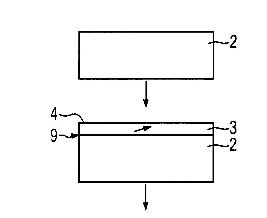
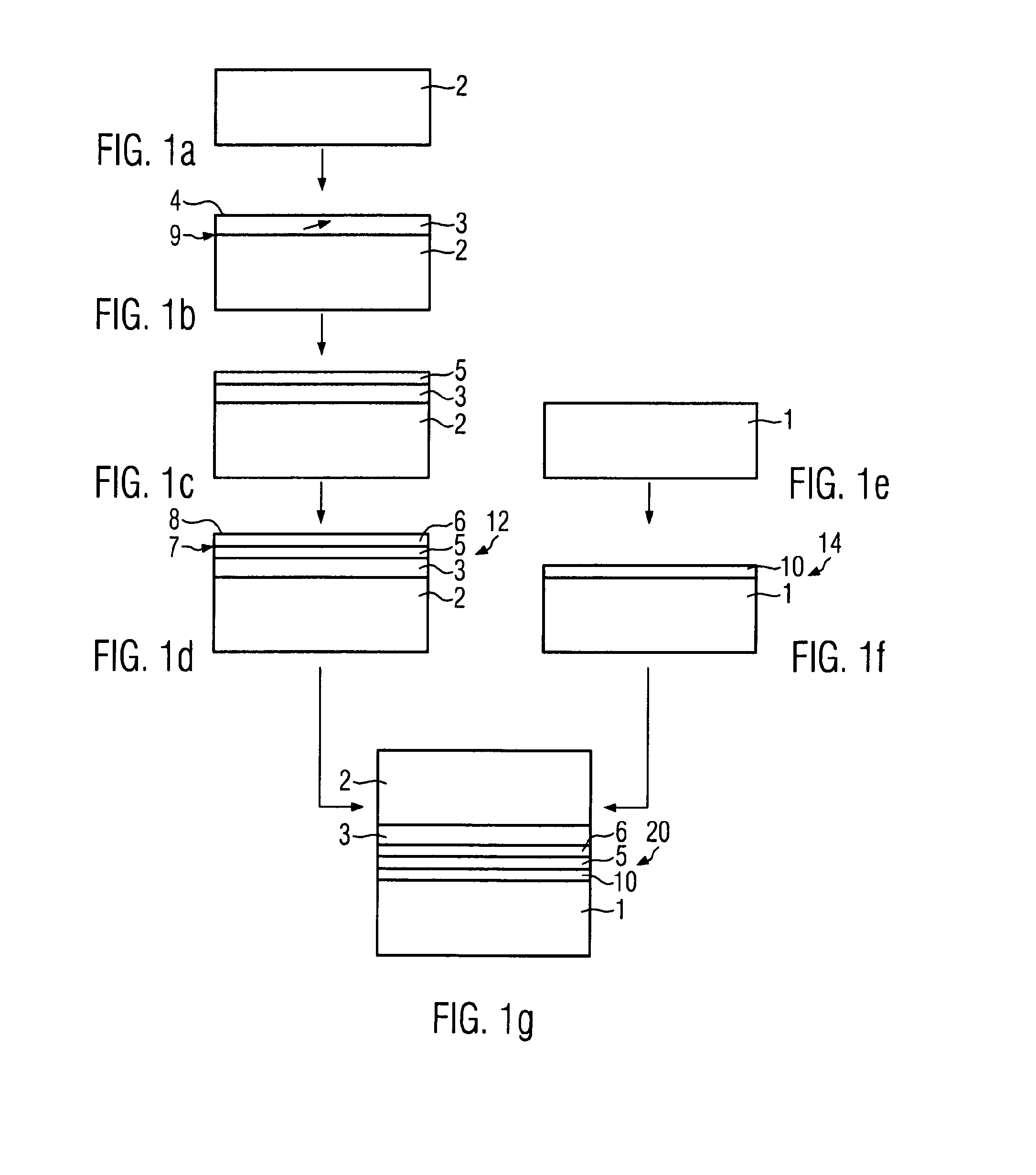
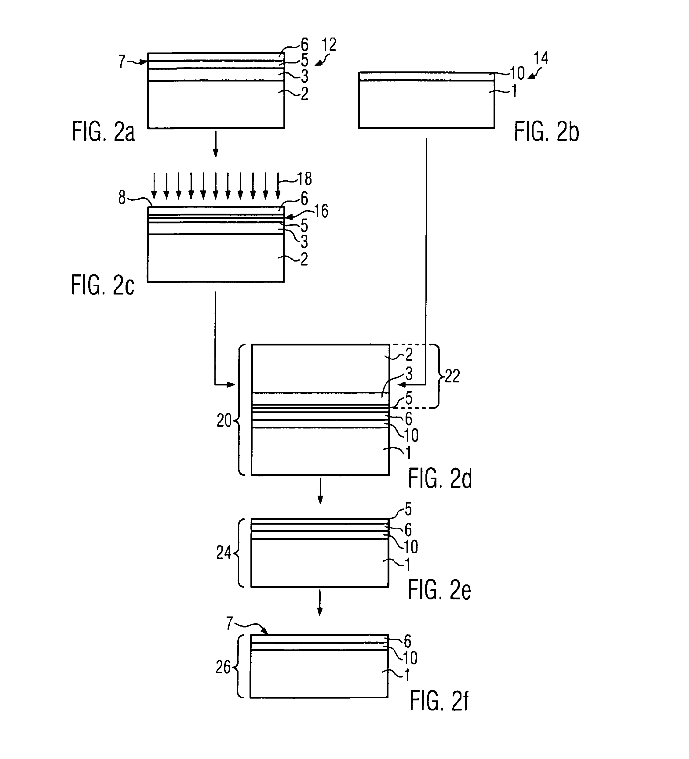
[0019]In this context, the term “in-plane lattice parameter” corresponds to a lattice parameter of the various layers in a direction essentially parallel to the interfaces between the various layers and to lattice parameters which the layers would show in an relaxed state. It is, in fact, known that the lattice parameter depends on the material used, but also on the nature of the underlying material on which it is deposited. To be able to compare lattice parameter values of different layers in the following, it is always referred to values as if the layers were in a relaxed state, and not in the strained state under heteroepitaxial conditions, which is also known under the terms pseudomorphic or commensurate growth. As an interface may be characterized by two lattice parameters, the above-mentioned condition can either be satisfied for both lattice parameters or for only one. In addition, the top layer of the heterostructure is not necessarily the final layer, further layers straine...


PUM


Abstract

A method for manufacturing a semiconductor heterostructure by first manufacturing a donor wafer having a first substrate with a first in-plane lattice parameter, a spatially graded buffer layer having a second in-plane lattice parameter, and a strained smoothing layer of a semiconductor material having a third in-plane lattice parameter which has a value between that of the first and second lattice parameters. A top layer is formed on the ungraded layer a top layer of a semiconductor material having a top surface, optionally with a superficial layer present on the top surface and having a thickness that is equal to or smaller than 10 nanometers. Next, a handle wafer of a second substrate having an insulator layer thereon is bonded with the donor wafer in such way that (a) the insulator layer of the handle wafer is bonded directly onto the top surface of the top layer of the donor wafer, or (b) the insulator layer of the handle wafer is bonded onto the superficial layer.

Description

BACKGROUND ART[0001]The invention relates to a method of manufacturing a semiconductor heterostructure, comprising manufacturing a donor wafer, comprising providing a first substrate with a first in-plane lattice parameter, providing on the first substrate an at least spatially graded buffer layer having on top in a relaxed state a second in-plane lattice parameter, forming on the graded buffer layer an ungraded layer of a semiconductor material having in relaxed state a third in-plane lattice parameter, forming on the ungraded layer a top layer of a semiconductor material, and manufacturing a handle wafer, comprising providing a second substrate, forming on the second substrate an insulator layer, and bonding the donor wafer with the handle wafer.[0002]Semiconductor heterostructures like this are used, for instance, to transfer the top layer or the top layer and a part of the ungraded layer by means of splitting of the donor wafer onto the handle wafer.[0003]A principal structure o...

Claims


Application Information

Patent Timeline
Patent Type & Authority Patents(United States)
IPC IPC(8): H01L21/00H01L21/302
CPCH01L21/76254H01L21/02381H01L21/0245H01L21/02532H01L21/0262H01L21/76256H01L21/20B82Y40/00
Inventor AULNETTE, CECILEFIGUET, CHRISTOPHEDAVAL, NICOLAS
Owner SOITEC SA
Why Eureka
Try Eureka