
Segmented on-chip memory and requester arbitration

a technology of requester arbitration and on-chip memory, which is applied in the field of control of access to on-chip memory, can solve the problems of high power consumption, severe power consumption, and lower capacity of dual-port ram devices, and achieve the effects of improving efficiency, simplifying manufacturing, and increasing overall operating speed

Active Publication Date: 2008-12-02
ADVANCED MICRO DEVICES INC
View PDF28 Cites 7 Cited by
  • Summary
  • Abstract
  • Description
  • Claims
  • Application Information

AI Technical Summary

Benefits of technology

This patent describes an improved memory access technique for WLAN devices that can compensate for interface latencies, increase operating speed, and improve efficiency without sacrificing performance. The WLAN communication device described in the patent includes an on-chip memory with multiple memory circuits forming individually-addressable memory segments, and an arbitration circuit that can determine which memory circuit to access based on the requests of multiple requesters. The memory device can also include a method for controlling access to the on-chip memory by receiving requests from multiple requesters and determining which memory segment to access based on the request. The technical effects of this patent include improved memory access speed and efficiency, reduced chip area-related costs, and power consumption without performance loss.

Problems solved by technology

However, dual-port RAM devices tend to have lower capacity, to need large chip areas, and to suffer from severe power consumption.
Thus, the existing convention techniques may have problems in that they either cannot provide the performance, operating speed and efficiency needed to comply with the requirements (in particular when using single-port devices), or they require high chip area and lead to high power consumption, thereby increasing the manufacturing and development costs (for instance when using dual-port devices or even multi-port units that have more than two ports).
Moreover, the prior art techniques are often much too inflexible to allow for meeting the data throughput constraints given by modern applications.
Thus, conventional techniques often do not allow for sufficiently compensating interface latencies.

Method used


Image

  • Segmented on-chip memory and requester arbitration
  • Segmented on-chip memory and requester arbitration
  • Segmented on-chip memory and requester arbitration

Examples


Embodiment Construction

[0028]The illustrative embodiments of the present invention will be described with reference to the figure drawings wherein like elements and structures are indicated by like reference numbers.

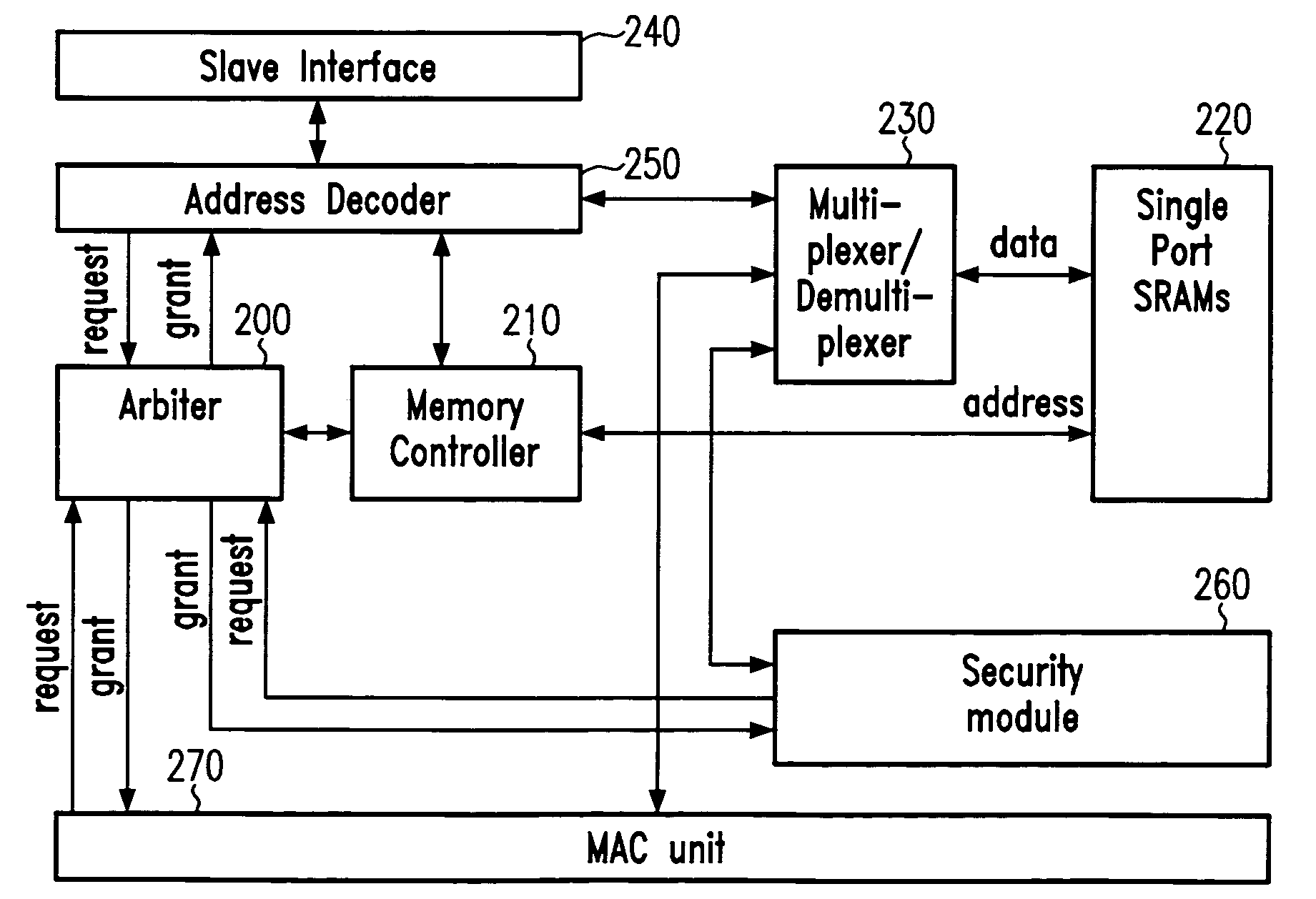
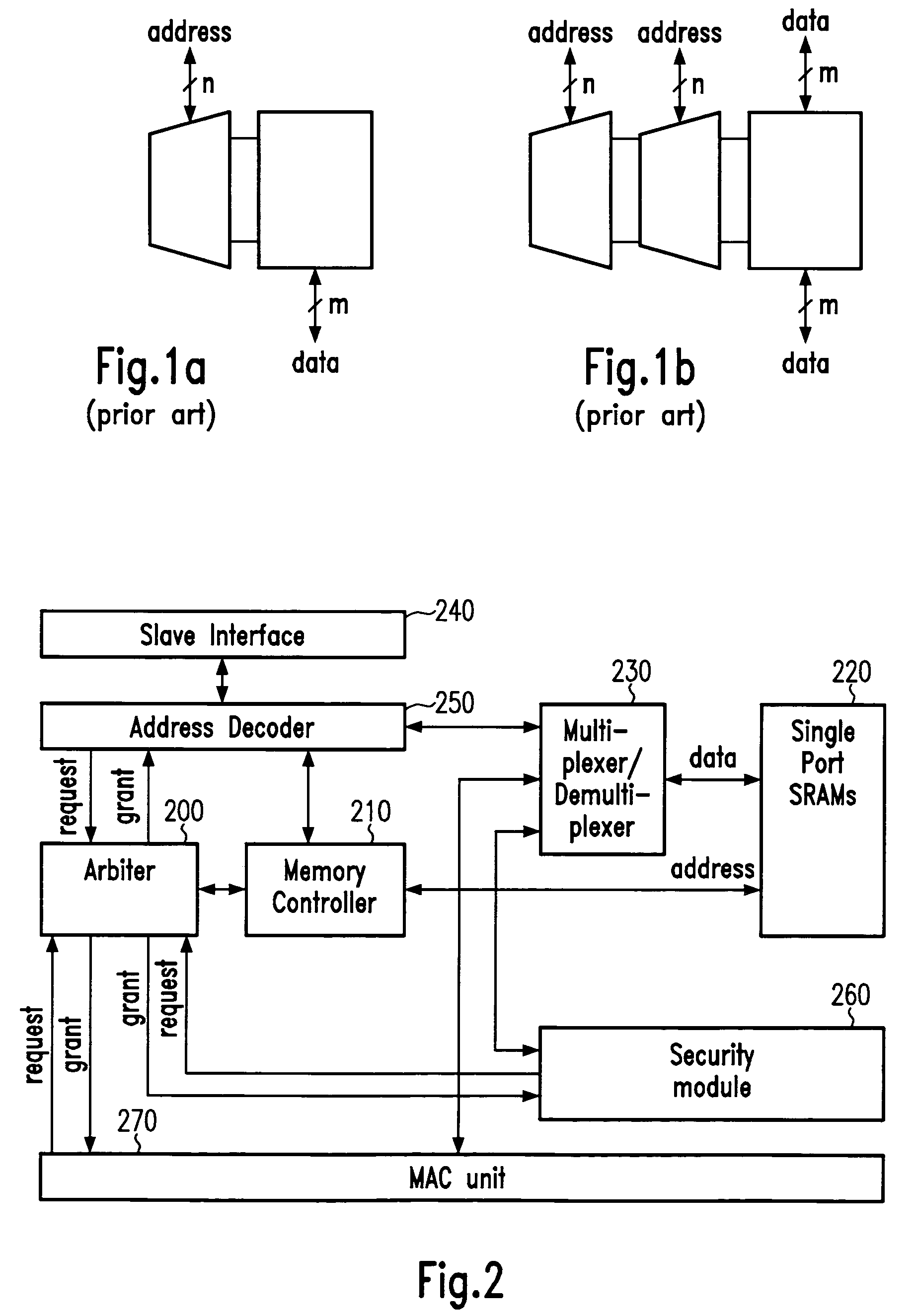
[0029]Referring now to FIG. 2, an arrangement is shown for controlling access to an on-chip memory 220 by multiple requesters 240, 250; 260; 270. As may be seen from FIG. 2, the on-chip memory 220 of the present embodiment is built from single-port SRAM devices. Unlike DRAM (Dynamic Random Access Memory), SRAM-type memory devices do not need to be periodically refreshed. Moreover, SRAM is faster than DRAM.

[0030]Since the on-chip memory 220 of the present embodiment is built from single-port memory devices, the chip area needed to implement this technique is significantly reduced. In addition, the power consumption may be reduced as well.

[0031]The single-port SRAM based on-chip memory 220 is shown in FIG. 2 to have a data port and an address port. The data port is connected to a multiplexer / dem...


PUM


Abstract

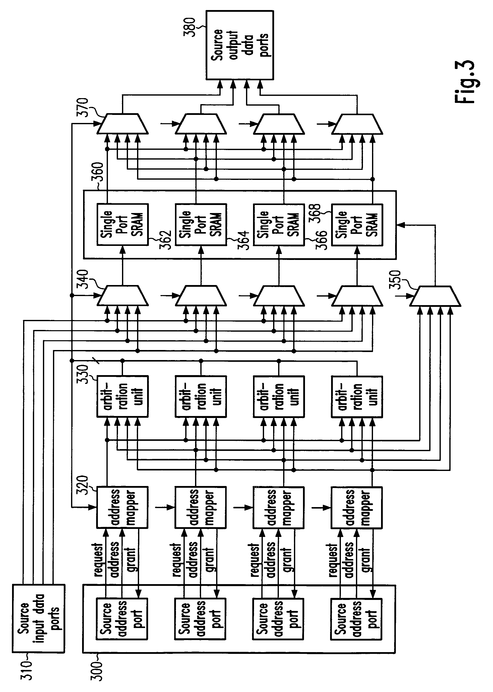
A memory access technique is provided that may be used in WLAN (Wireless Local Area Network) communication devices. An on-chip memory has multiple memory circuits forming individually addressable memory segments. An arbitration unit arbitrates between multiple requesters, each requesting access to the on-chip memory. The requesters are on-chip circuits and / or external devices. The arbitration unit determines a memory circuit to be accessed for each request that is received from a requester. The determination may be based on a software configurable arbitration scheme. The memory segments may form a bank of single-port SRAM (Static Random Access Memory) devices.

Description

BACKGROUND OF THE INVENTION[0001]1. Field of the Invention[0002]The invention generally relates to WLAN (Wireless Local Area Network) communication devices, integrated circuit chips, memory devices and corresponding methods, and more particularly to techniques for controlling access to an on-chip memory.[0003]2. Description of the Related Art[0004]A wireless local area network is a flexible data communication system implemented as an extension to or as an alternative for a wired LAN. Using radio frequency or infrared technology, WLAN systems transmit and receive data over the air minimizing the need for wired connections. Thus, WLAN systems combine data connectivity with user mobility.[0005]Today, most WLAN systems use spread spectrum technology, a wideband radio frequency technique developed for use in reliable and secure communication systems. The spread spectrum technology is designed to trade-off bandwidth efficiency for reliability, integrity and security. Two types of spread s...

Claims


Application Information

Patent Timeline
Patent Type & Authority Patents(United States)
IPC IPC(8): G06F12/00H04Q7/24
CPCG06F13/1605Y10S370/913Y02B60/1228Y02D10/00
Inventor BAER, MATTHIASTISCHER, FALKGOETTING, OLIVERSCHLEGEL, PEER
Owner ADVANCED MICRO DEVICES INC
Learn More