
Inorganic resist material and nano-fabrication method by utilizing the same

Inactive Publication Date: 2008-12-16
IND TECH RES INST
View PDF7 Cites 14 Cited by
  • Summary
  • Abstract
  • Description
  • Claims
  • Application Information

AI Technical Summary

Benefits of technology

[0011]The inorganic resist material of the present invention is a heat-sensitive material, so merely the region having a temperature higher than the phas

Problems solved by technology

However, even a small amount of photons can also cause a change in the chemical structure of the organic photoresist to some extent.
Furthermore, the organic resist material is a polymer material, so after exposure and development, the edges of the patterns or the recording pits are likely to be rough, and fine line patterns or recording pits in the level of several nanometers are difficult to be fabricated.
However, the fabrication cost is increased significantly due to the problems such as short-wavelength laser is used and the optical elements of the exposure mechanism must be made of specific materials, and the problem that the edges of patterns or the recording pits become rough after exposure and development cannot be solved.
Though such techniques can meet the requirements of reaching the accuracy of several nanometers, the problems of slow process and high cost still exist.

Method used


Image

  • Inorganic resist material and nano-fabrication method by utilizing the same
  • Inorganic resist material and nano-fabrication method by utilizing the same
  • Inorganic resist material and nano-fabrication method by utilizing the same

Examples


experimental example (

3)

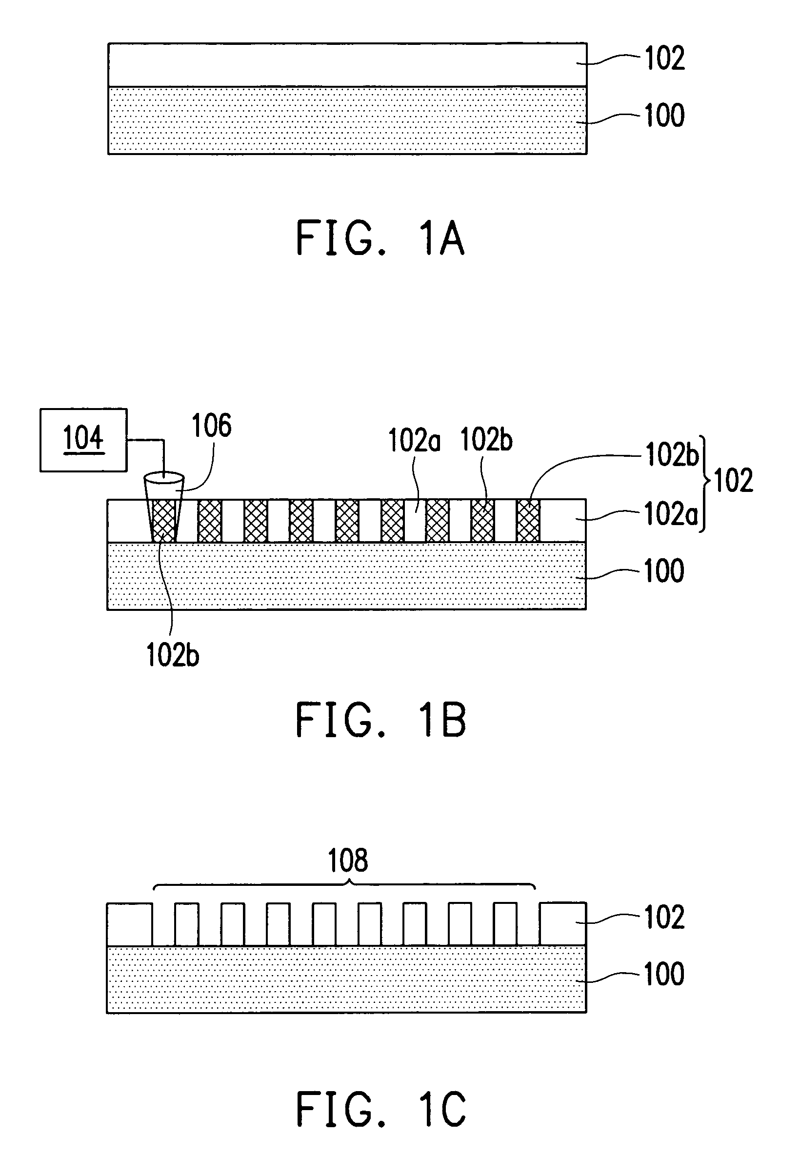
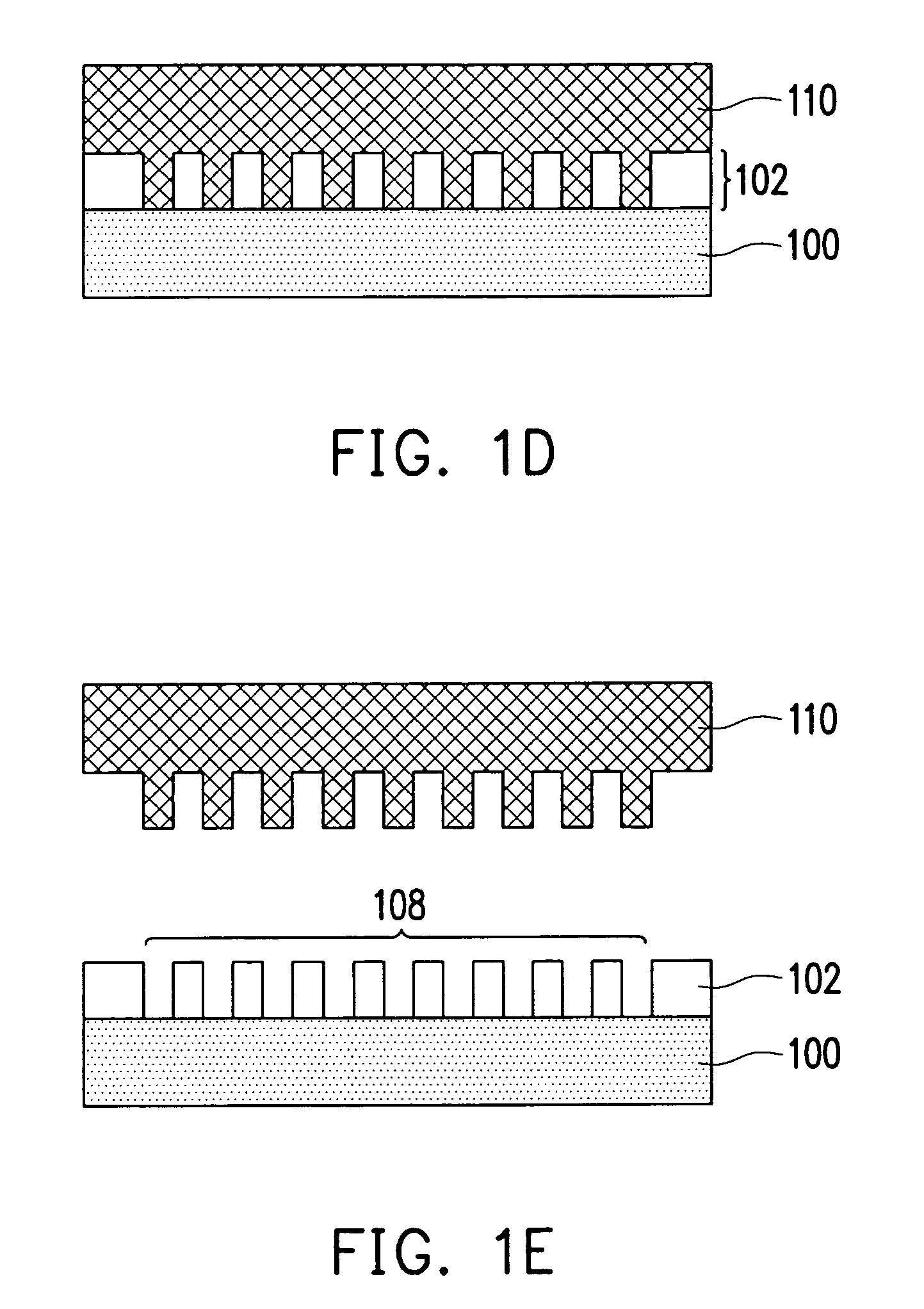
[0061]A ZnS—SiO2 layer having a thickness of 70 nm is coated on a PC substrate of a DVD-RW by vacuum sputtering, and an incomplete oxide of a phase-change material (Ge—Sb—Sn) is coated on the ZnS—SiO2 layer by oxygen reactive sputtering, in which the thickness of the incomplete oxide of the phase-change material (Ge—Sb—Sn) is approximately 65 nm. The flow ratio of Ar and O2 is 10:3 during coating the incomplete oxide of the phase-change material (Ge—Sb—Sn). In this experimental example, the wavelength of the exposure device is 405 nm, the numerical aperture is NA=0.65, rotation speed of the substrate is 6.6 m / s, the laser is output in the manner of DC output, and samples under exposure laser powers of 2.5 mW, 2.75 mW, and 3 mW are respectively prepared according to different exposure laser powers. The alkali solution for removing the phase transition part is a KOH solution, and the removal time is 60 seconds.

[0062]The results of the experimental example (3) are as shown in the acc...


PUM


Abstract

An inorganic resist material is provided, which is an incomplete oxide of a phase-change material. The oxygen content in the inorganic resist material is lower than the stoichiometric oxygen content of a complete oxide of the phase-change material, and a general formula of the inorganic resist material is A1-xOx, in which A represents the phase-change material, and x is between 5 at. % and 65 at. %. The inorganic resist material can be used to form line patterns or recording pits with size smaller than the exposure light spot by using the laser of conventional lithography process as an exposure source.

Description

CROSS-REFERENCE TO RELATED APPLICATION[0001]This application claims the priority benefit of Taiwan application serial no. 96130337, filed Aug. 16, 2007. The entirety of the above-mentioned patent application is incorporated herein by reference and made a part of this specification.BACKGROUND OF THE INVENTION[0002]1. Field of the Invention[0003]The present invention relates to a nano-fabrication method, and more particularly, to an inorganic resist material and a nano-fabrication method by utilizing the same.[0004]2. Description of Related Art[0005]With the rapid development of 3C science and technology, it is necessary for the semiconductor process and information recording media process to reduce line width or the size of recording pit, so as to improve the operation speed and the recording density. Taking optical disc storage as an example, the length of the minimum recording pit of DVD discs is approximately 400 nm, and the length of the minimum recording pit of the next generati...

Claims


Application Information

Patent Timeline
IPC IPC(8): G03F7/00G03F7/004
CPCB82Y10/00B82Y40/00G03F7/0002G03F7/0043G11B7/261
Inventor CHEN, JUNG-POHSU, MING-FANGLEE, AN-TSECHENG, CHUNG-TAYANG, CHIN-TIENCHANG, SHENG-LICHIU, KUO-CHI
Owner IND TECH RES INST
Learn More