Multi-port dynamic memory structures

a dynamic memory and multi-port technology, applied in the field of dynamic memory, can solve the problems of reducing the availability of the memory array for normal read and write operations, reducing the overall system performance, and reducing the availability of the memory array for normal operations

Active Publication Date: 2008-12-16
GLOBALFOUNDRIES U S INC
View PDF14 Cites 11 Cited by
  • Summary
  • Abstract
  • Description
  • Claims
  • Application Information

AI Technical Summary

Problems solved by technology

During refreshing of the memory cells, the memory array that contains the cells being refreshed is suspended from the normal read and write operations, thereby reducing the availability of the memory array for normal read and write operations and, hence, potentially reducing the overall system performance.
The more often the memory array needs to be refreshed (i.e., the shorter the retention time), the lower the availability of the memory array for normal operations and potentially the lower the overall system performance.
The device variability of semiconductor technology has become a major issue as the minimum feature size approaches the physical limits.
This leads to the instability of, for example, 6T SRAM cells, which limits the scaling of the cells.
That is, if a refresh cycle were “hidden,” it would not prevent the carrying out of a read or write operation, as the case may be, during the “hidden” refresh.

Method used


Image

  • Multi-port dynamic memory structures
  • Multi-port dynamic memory structures
  • Multi-port dynamic memory structures

Examples


case 1 (read and write scheduling , flow-chart 1300 of fig.13a)

[0063]Case 1 (Read and Write Scheduling, Flow-Chart 1300 of FIG. 13A)

case 1.0

[0064

[0065]If the read address is not the same as the write address (“no” branch of decision block 1302), then the following operations are performed, at block 1306:[0066](1) Activate the wordline WLr to perform a read operation;[0067](2) Activate the wordline WLw to perform a write operation.

case 1.1

[0068

[0069]If the read address is the same as the write address during the current cycle (“yes” branch of decision block 1302), then the following operations are performed, at block 1304:

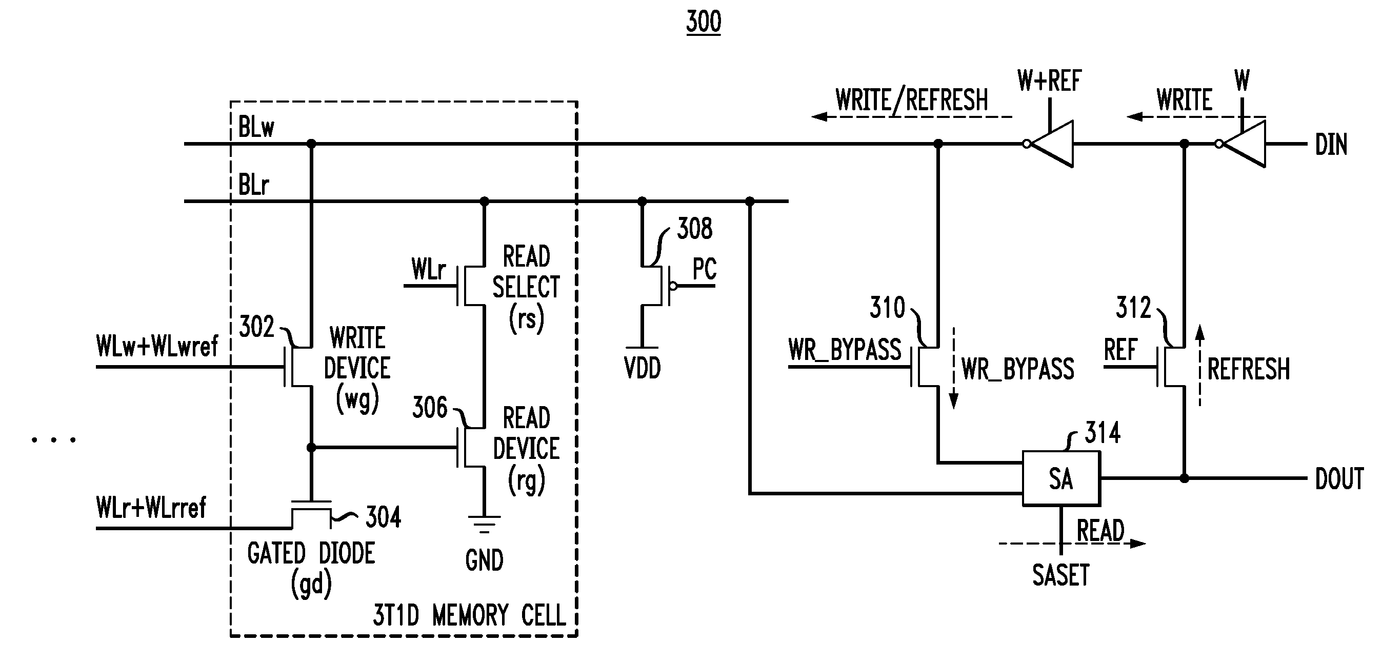
[0070]the wordline WLr is not activated as there is no read of the stored data. The write-read bypass (WR_BYPASS) FET 408, 508, 608, 708, coupling the write data path and the read data path, is activated to pass the new data for the write operation directly to the sense amplifier 414, 514, 614, 714, without reading from DMC. The new data is then written to the memory array by activating the WLw+WLwref control signal.

[0071]The method of scheduling under the different address conditions for read and write operations is thus summarized in FIG. 13A in the form of flow-chart 1300.


PUM


Abstract

A dynamic random access memory circuit has at least one write bit line, at least one read bit line, a capacitive storage device, a write access device operatively coupled to the capacitive storage device and the at least one write bit line, a sense amplifier operatively coupled to the at least one read bit line and configured to generate an output signal, and a refresh bypass device operatively associated with the sense amplifier and the at least one write bit line so as to selectively pass the output signal to the at least one write bit line.

Description

FIELD OF THE INVENTION[0001]The present invention relates to electronic circuits and, more particularly, relates to dynamic memory.BACKGROUND OF THE INVENTION[0002]In dynamic random access memory (DRAM) cells, such as the 1T1C cell, the 3T (or 3T1C) gain cell, and the gated diode cells, 0- and 1-data are stored as electric charges in various storage elements, such as a stack capacitor, trench capacitor, transistor gate capacitor, and gated diode. The stored charges can only remain in the storage element for a finite amount of time, as there are leakage paths from the storage node, which holds the charges, to the neighboring nodes. Typical leakage paths are the source-drain path of the write device under sub-threshold leakage, the tunneling leakage through the storage element oxide and the gate oxide of the write device and the read device (as in the case for the 3T, 3T1C, 3T1D and 2T1D cells, for example), and the storage node to silicon body leakage via the junction leakage of the ...

Claims


Application Information

Patent Timeline
Patent Type & Authority Patents(United States)
IPC IPC(8): G11C11/34
CPCG11C7/12G11C7/18G11C8/16G11C11/403G11C11/405G11C11/406G11C11/40615G11C11/4094G11C11/4097G11C2211/4065G11C11/40603G11C11/40607G11C11/4076G11C2207/2209G11C8/18
Inventor LUK, WING K.JI, BRIAN L.
Owner GLOBALFOUNDRIES U S INC
Why Eureka
Try Eureka