Solid-state image sensor
a solid-state image and sensor technology, applied in the direction of electrical equipment, semiconductor devices, radio frequency controlled devices, etc., can solve the problems of contaminated metal intensively, insufficient gettering capability in the pixel region, and degradation of device characteristics such as dark output, so as to achieve effective gettering and eliminate contamination
- Summary
- Abstract
- Description
- Claims
- Application Information
AI Technical Summary
Benefits of technology
Problems solved by technology
Method used
Image
Examples
first embodiment
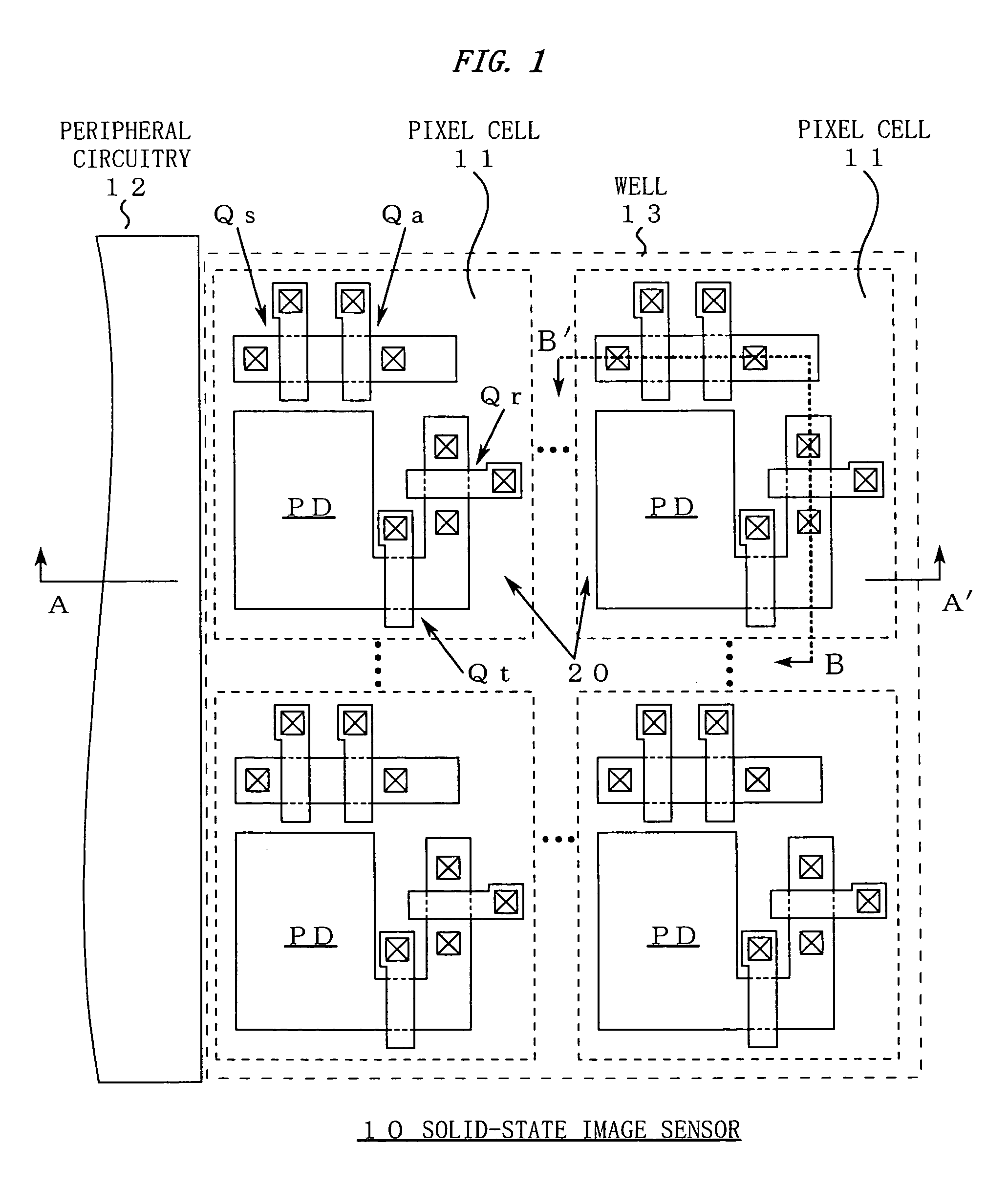
[0026]FIG. 1 is a view showing the configuration of a light-receiving face of a solid-state image sensor 10.
[0027]As shown in FIG. 1, the solid-state image sensor 10 generally includes pixel cells 11 arranged in an array and peripheral circuitry 12 having a vertical scan circuit or the like. The plurality of pixel cells 11 are formed inside a well 13.
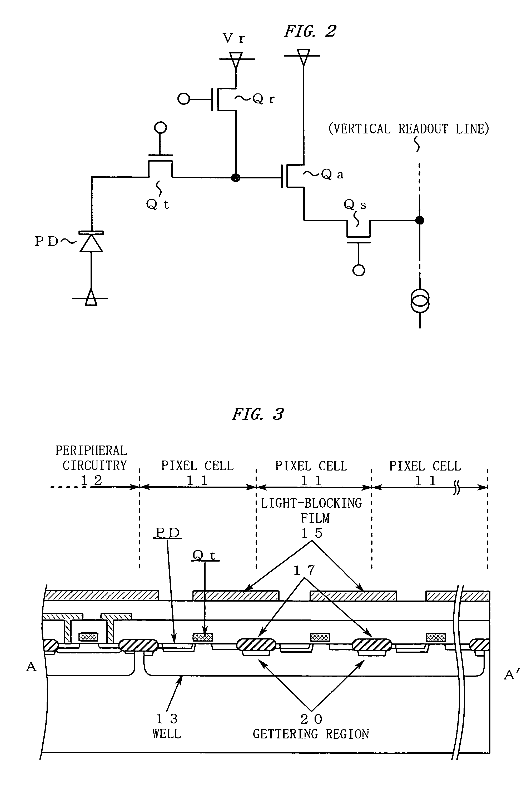
[0028]FIG. 2 is a view showing an equivalent circuit of the pixel cell 11.
[0029]The pixel cell 11 has the following elements formed therein by patterning:
(1) A photodiode PD for photoelectric conversion of incident light into signal charges;
(2) A MOS switch Qr for reset operations;
(3) A MOS switch Qt for reading signal charges from the photodiode PD;
(4) An amplification element Qa for converting the read signal charges into a voltage signal; and
(5) A MOS switch Qs for selecting an output row.
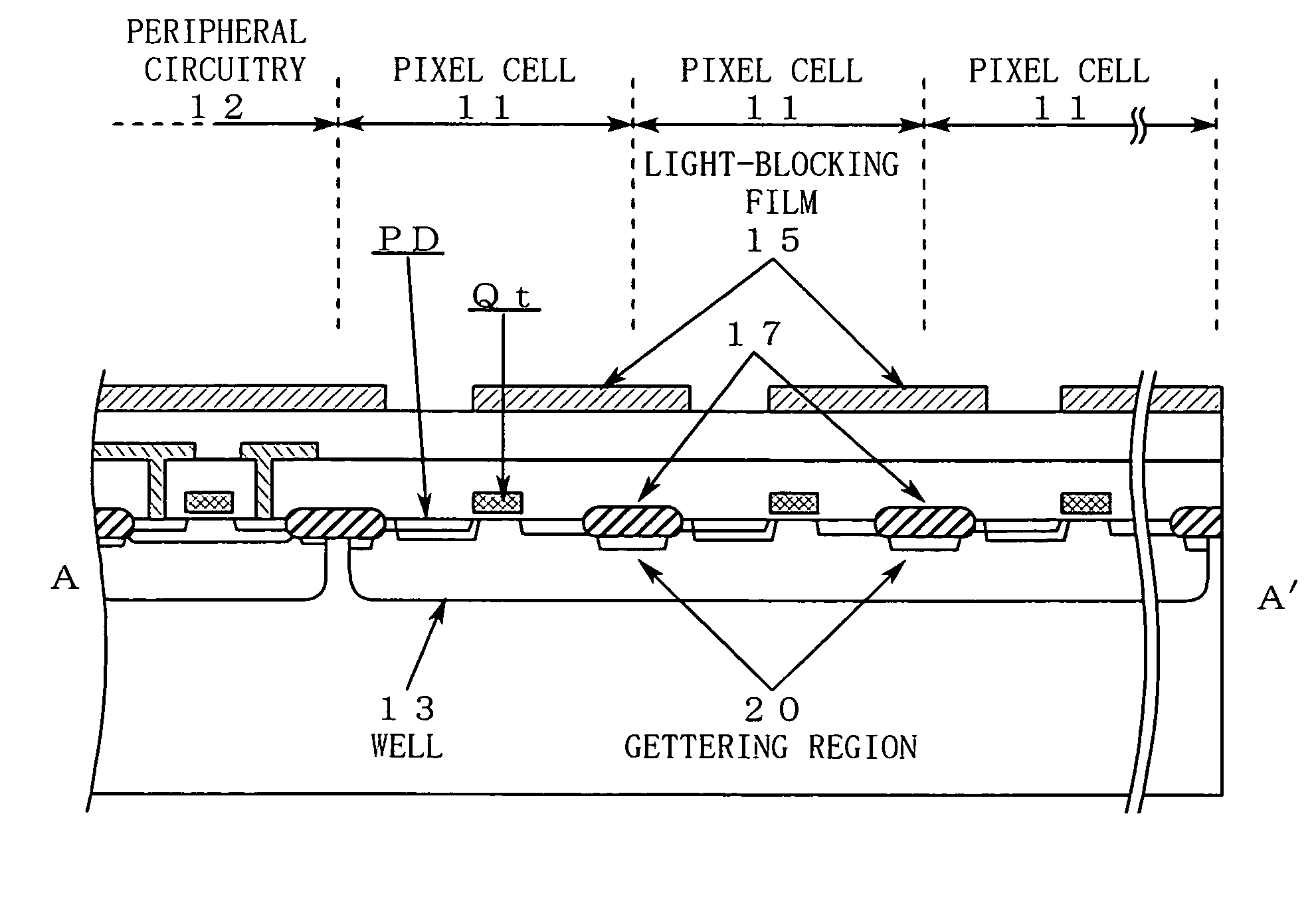
[0030]FIG. 3 is a cross-sectional view taken along the line A-A′ shown in FIG. 1.
[0031]As shown in FIG. 3, the surface of the pixel cells 11 is cov...
second embodiment
[0041]The structure of a pixel cell according to the second embodiment is the same as that of the first embodiment (FIGS. 1 and 2), and thus will not be repeatedly described.
[0042]FIG. 4 is a cross-sectional view taken along the line B-B′ shown in FIG. 1.
[0043]As shown in FIG. 4, in the second embodiment, a gettering region 20a is provided in the region of the MOS switch Qr (to which a reset voltage is applied), the drain region of the amplification element Qa, and the region of the MOS switch Qs (which is connected to the vertical readout line). In particular, one of these regions which is in ohmic contact with the metal conductor may also be referred to as a contact region to distinguish it from the gettering region which is not in ohmic contact with the metal conductor. In these gettering regions 20a, an impurity such as phosphorus is introduced with an average impurity concentration of 1E20 cm−3 or more.
[0044]Also, inside the gettering region 20a lattice defects such as dislocat...
third embodiment
[0049]FIG. 5 is a view showing the configuration of a light-receiving face of a solid-state image sensor 30.
[0050]As shown in FIG. 5, the solid-state image sensor 30 includes pixel cells 41 arranged in an array and peripheral circuitry 42 having a vertical scan circuit or the like.
[0051]FIG. 6 is a view showing an equivalent circuit of the pixel cell 41.
[0052]The pixel cells 41 are patterned with a photodiode PD for photoelectric conversion of incident light into signal charges, a MOS switch Qt for reading signal charges from the photodiode PD, a MOS switch Qr for reset operations, and an amplification element Qa of a junction type FET for converting the read signal charges into a voltage signal.
[0053]FIG. 7 is a cross-sectional view taken along the line C-C′ shown in FIG. 5.
[0054]FIG. 8 is a cross-sectional view taken along the line D-D′ shown in FIG. 5.
[0055]As shown in FIGS. 7 and 8, in the third embodiment, gettering regions 32a and 33a are provided on a main electrode 32 of the...
PUM
 Abstract
Description
Claims
Application Information


