Input receiver circuit

a receiver circuit and input receiver technology, applied in the direction of generating/distributing signals, pulse techniques, instruments, etc., can solve the problems of increasing the cost of purchase and operation of serial-to-parallal converters, increasing the cost of serial-to-parallal converters, and increasing the cost of bit errors, so as to reduce the susceptibility to bit errors, low development and production effort, and high transmission speed

Active Publication Date: 2009-01-13
CHANGXIN MEMORY TECH INC
View PDF11 Cites 21 Cited by
  • Summary
  • Abstract
  • Description
  • Claims
  • Application Information

AI Technical Summary

Benefits of technology

[0023]Another advantage of the present invention is that the inventive method of receiving a high-speed input signal has a lower susceptibility to bit errors and is thus also suitable in particular for a transmission of data and clock over the same channel.
[0024]A preferred application of the present invention is in data memories or memory devices for computer and other applications. The present invention is particularly applicable in a DRAM, SRAM, flash or also in another memory and in particular at the input side thereof, in order to receive a high-speed signal. The high-speed signal transmits, for example, data to be stored in the data memory, an address of a memory location in the data memory or a control signal for the data memory. The high-speed signal is received according to the present invention. In response to the high-speed signal, a plurality of output signals is output, which are processed by the data memory. This processing involves, for example, storing or reading out data, and both data to be stored and the address of a memory location in the data memory in which the data are to be stored or from which the data are to be read out and the control instructions for storing or reading out the data can be transmitted by the high-speed signal. The present invention enables also in this application a high transmission speed with a low development and production effort, and also offers low susceptibility to bit errors even in the case of a highly noisy or otherwise highly disturbed input signal.
[0025]According to a preferred embodiment of the present invention, the integration elements are capacitors charged by the input signal via a resistor. Alternatively, instead of the resistor a current source that can be controlled by the input signal is provided.

Problems solved by technology

However, the shorter setup and hold time of a circuitry are, the higher the development effort, production costs and power requirements thereof are as a rule.
One disadvantage of the conventional serial-to-parallel converter illustrated by using FIG. 3 is thus that an increase of the transmission rate results in an increase of the costs of purchase and operation of the serial-to-parallel converter.
In addition to that, the conventional serial-to-parallel converter illustrated by using FIG. 3 comprises a marked tendency towards bit errors, in particular when data and clock are transmitted over the same channel or when the input signal is noisy or has a high noise level.
However, in many applications, namely in high-speed applications, the input signal has a high noise level.
The conventional serial-to-parallel converter illustrated in FIG. 3 is thus hardly suitable for receiving high-speed input signals or not at all.
If at all, it is only adaptable to a high-speed application with a high effort in terms of circuit engineering and at the cost of high supply power requirements.
However, some of the development efforts, the production costs and the supply power requirements can be attributed to these properties.

Method used


Image

  • Input receiver circuit
  • Input receiver circuit
  • Input receiver circuit

Examples


Embodiment Construction

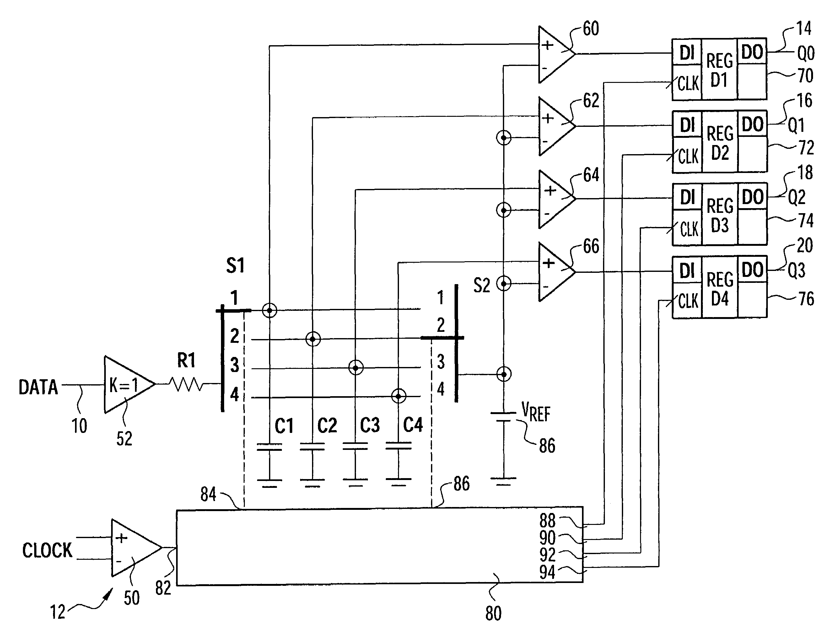
[0030]FIG. 1 is a schematic circuit diagram showing an input receiver circuit according to a preferred embodiment of the present invention. The inventive input receiver circuit includes an input 10 for receiving an input signal data and a clock signal input 12 for receiving an input clock signal clock. Preferably, the input signal is a high-speed input signal or an input signal having a high transmission rate. Further the inventive input receiver circuit includes outputs 14, 16, 18, 20 for outputting output signals Q0, Q1, Q2, Q3 in parallel. The clock signal input 12 is herein illustrated by way of example with an differential amplifier or comparator 50 whose two inputs +, − receive complementary signals or signals 1800 out of phase with respect to one another which together form the input clock signal clock.

[0031]The input 10 is connected to an amplifier having the gain K=1 or to a sequential circuit 52. The input signal buffered by the sequential circuit 52 is fed to a switch S1 ...


PUM


Abstract

An input receiver circuit is provided for receiving a noisy high-speed input signal and for generating a plurality of output signals that can be processed at a low acquisition speed compared to the speed of the high-speed input signal. The input receiver circuit includes an input for receiving the high-speed input signal (data), a plurality of integration elements and a switch for connecting the input to one of the plurality of integration elements for integrating the high-speed input signal. The input receiver circuit further includes a plurality of means for receiving one of the integrated high-speed input signals at a time and for outputting one of the plurality of output signals at a time, and a controller for controlling the switch.

Description

BACKGROUND OF THE INVENTION[0001]1. Field of the Invention[0002]The present invention relates to an input receiver circuit for receiving a high-speed input signal representing one datum of a plurality of data in each of successive input clock intervals and for outputting a plurality of output signals which can be processed at a lower acquisition speed compared to the speed of the high-speed input signal, and each of which represents one datum of the plurality of data within an output clock interval.[0003]2. Description of the Related Art[0004]In numerous applications, in particular in data transmission, data storage and data processing, data serially coded by an input signal with a high-speed or transfer speed or data transfer rate have to be received and processed. In doing so, it is often desirable to acquire and process further the data with an acquisition speed lower than the transmission speed of the input signal.[0005]For this purpose, a serial-to-parallel converter is convent...

Claims


Application Information

Patent Timeline
Patent Type & Authority Patents(United States)
IPC IPC(8): H03M9/00G06F1/04H03K5/15
CPCH03M9/00
Inventor KUZMENKA, MAKSIMRUCKERBAUER, HERMANN
Owner CHANGXIN MEMORY TECH INC
Why Eureka
Try Eureka