Method of forming a ZrO2 thin film using plasma enhanced atomic layer deposition and method of fabricating a capacitor of a semiconductor memory device having the thin film

a semiconductor memory device and atomic layer deposition technology, applied in the direction of coatings, solid-state devices, chemical vapor deposition coatings, etc., can solve the problems of leakage current deterioration and need to be developed, and achieve the effects of improving electrical characteristics, shortening the deposition cycle time, and improving deposition speed

Inactive Publication Date: 2009-02-17
SAMSUNG ELECTRONICS CO LTD
View PDF18 Cites 13 Cited by
  • Summary
  • Abstract
  • Description
  • Claims
  • Application Information

AI Technical Summary

Benefits of technology

[0009]In example embodiments of the present invention, a method of forming a ZrO2 thin film may be formed at a higher deposition speed to improve productivity and may be employed as a capacitor dielectric layer of a semiconductor device to provide improved electrical characteristics. In other example embodiments of the present invention, a method of fabricating a capacitor of a semiconductor memory device may employ a dielectric layer having improved thermal characteristics and / or electrical characteristics. The method of fabricating a capacitor of a semiconductor memory device may still keep leakage current characteristics stable to increase (if not maximize) a capacitance.
[0012]According to example embodiments of the present invention, a ZrO2 thin film, having improved electrical characteristics, may be formed with a higher deposition speed and / or a shorter deposition cycle time. By employing the ZrO2 thin film as a capacitor dielectric layer of a semiconductor device, a capacitor may be fabricated with an increased (if not maximized) capacitance, while its leakage current characteristics may be maintained.

Problems solved by technology

Because the MIS structure using a SiO2 dielectric layer has reached procedural limitations with increased integration of the device, new technology may need to be developed.
HfO2 may be crystallized at a temperature of about 450° C., which may cause deterioration of leakage current characteristics.

Method used


Image

  • Method of forming a ZrO2 thin film using plasma enhanced atomic layer deposition and method of fabricating a capacitor of a semiconductor memory device having the thin film
  • Method of forming a ZrO2 thin film using plasma enhanced atomic layer deposition and method of fabricating a capacitor of a semiconductor memory device having the thin film
  • Method of forming a ZrO2 thin film using plasma enhanced atomic layer deposition and method of fabricating a capacitor of a semiconductor memory device having the thin film

Examples


Embodiment Construction

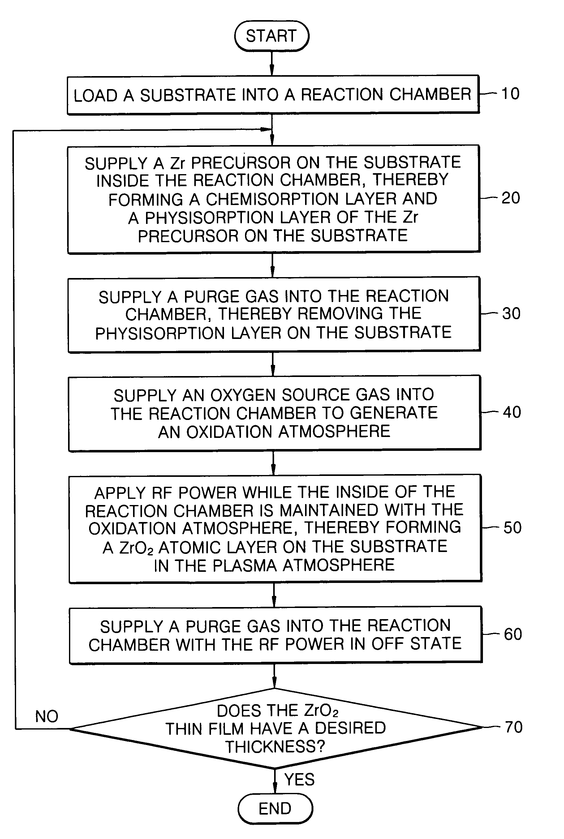
[0027]Various example embodiments of the present invention will now be described more fully with reference to the accompanying drawings, in which some example embodiments of the invention are shown. This invention may, however, be embodied in many alternate forms and should not be construed as being limited to only the embodiments set forth herein. Rather, these embodiments are provided so that this disclosure will be thorough and complete, and will fully convey the scope of the invention to those skilled in the art. Like numbers refer to like elements throughout the specification. In the drawings, the thicknesses of layers and regions are exaggerated for clarity.

[0028]As used herein, the term “and / or” includes any and all combinations of one or more of the associated listed items. It will be understood that when an element or layer is referred to as being “formed on” another element or layer, it can be directly or indirectly formed on the other element or layer. That is, for exampl...


PUM

PropertyMeasurementUnit
temperatureaaaaaaaaaa
RF poweraaaaaaaaaa

Abstract

Example embodiments of the present invention relate to a method of forming a dielectric thin film and a method of fabricating a semiconductor memory device having the same. Other example embodiments of the present invention relate to a method of forming a ZrO2 thin film and a method of fabricating a capacitor of a semiconductor memory device using the ZrO2 thin film as a dielectric layer. A method of forming a ZrO2 thin film may include supplying a zirconium precursor on a substrate maintained at a desired temperature, thereby forming a chemisorption layer of the precursor on the substrate. The zirconium precursor may be a tris(N-ethyl-N-methylamino)(tert-butoxy) zirconium precursor. The substrate having the chemisorption layer of the precursor may be exposed to the plasma atmosphere of oxygen-containing gas for a desired time, thereby forming a Zr oxide layer on the substrate, and a method of fabricating a capacitor of a semiconductor memory device having the ZrO2 thin film.

Description

PRIORITY STATEMENT[0001]This application claims priority under 35 U.S.C. § 119 to Korean Patent Application No. 10-2005-0064554, filed on Jul. 16, 2005, in the Korean Intellectual Property Office (KIPO), the entire contents of which are incorporated herein by reference.BACKGROUND[0002]1. Field[0003]Example embodiments of the present invention relate to a method of forming a dielectric thin film and a method of fabricating a semiconductor memory device having the same. Other example embodiments of the present invention relate to a method of forming a ZrO2 thin film and a method of fabricating a capacitor of a semiconductor memory device using the ZrO2 thin film as a dielectric layer.[0004]2. Description of the Related Art[0005]Highly integrated semiconductor memory devices may have a reduced design rule and an area may also be reduced that is occupied by a unit memory cell of the semiconductor memory device. An area may be reduced that is occupied by a capacitor used in a memory cell...

Claims


Application Information

Patent Timeline
Patent Type & Authority Patents(United States)
IPC IPC(8): H01L21/20H01L21/31H01L21/469
CPCC23C16/405C23C16/45542C23C16/45553C23C16/515H01L21/3141H01L21/31641H01L28/40H01L27/1085H01L21/02189H01L21/022H01L21/0228H10B12/03H01L21/20
Inventor SONG, MIN-WOOWON, SEOK-JUNKIM, WEON-HONGKWON, DAE-JINPARK, JUNG-MIN
Owner SAMSUNG ELECTRONICS CO LTD
Why Eureka
Try Eureka