Electronic device

a multi-layer ceramic and capacitor technology, applied in the direction of fixed capacitors, natural mineral layered products, electrical apparatuses, etc., can solve the problems of deterioration of reliability, thin dielectric ceramic layers and internal electrode layers, and inability to obtain high capacity, etc., to achieve superior temperature characteristics, superior dielectric constant or other electrical characteristics, and high reliability

Active Publication Date: 2009-05-05
TDK CORPARATION
View PDF28 Cites 18 Cited by
  • Summary
  • Abstract
  • Description
  • Claims
  • Application Information

AI Technical Summary

Benefits of technology

[0010]The present invention was made in consideration of this actual situation and has as its object the provision of a small sized, large capacity multilayer ceramic capacitor or other electronic device superior in dielectric constant or other electrical characteristics, superior in temperature characteristic even when making the dielectric layers thin, and high in reliability.
[0011]The inventors discovered that even when the dielectric layers are reduced in thickness to for example 5 μm or less or 3 μm or less, it is possible to control the thickness of the crystal grain boundaries between the crystal grains forming the dielectric layers to a suitable value so as to obtain a small sized, large capacity multilayer ceramic capacitor or other electronic device which satisfies the JIS B characteristic and EIA X5R characteristic and gives a high reliability and thereby completed the present invention.

Problems solved by technology

However, to obtain a small sized, high capacity multilayer ceramic capacitor, the dielectric ceramic layers and internal electrode layers have to be made thin.
Along with this, however, the reliability ends up deteriorating.
On the other hand, to obtain a small sized, high reliability multilayer ceramic capacitor, the dielectric ceramic layers and internal electrode layers have to be made thin, but with this a high capacity cannot be obtained.
However, with the method shown in this Document 1, for example, when making the dielectric ceramic layers a thin 3 μm or less, it is not always possible to obtain a reliability satisfying the demands of the market.
When making the dielectric ceramic layers a thin 3 μm or less, a reliability satisfying the demands of the market probably cannot be obtained.
For example, in Document 2, Mn or Mg or another sub ingredient is added in a very large amount, but if excessively adding an additive composition, donor or acceptor ingredients segregate at the crystal grain boundaries etc. and therefore the multilayer ceramic capacitor probably drops in reliability.
That is, with the method described in this Document 2, when making the dielectric layers thinner, problems such as an increase in insulation defects or a drop in the lifetime or other aspects of reliability are expected.
However, with the methods described in these patent documents, there is a large deterioration in the capacity with respect to the DC voltage and the demands of the market are not sufficiently satisfied.

Method used


Image

  • Electronic device
  • Electronic device
  • Electronic device

Examples


first embodiment

Method of Production of Multilayer Ceramic Capacitor

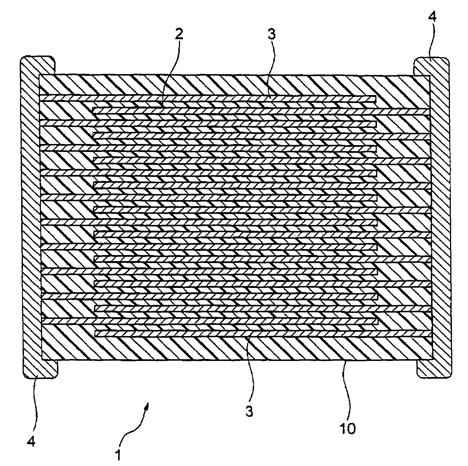
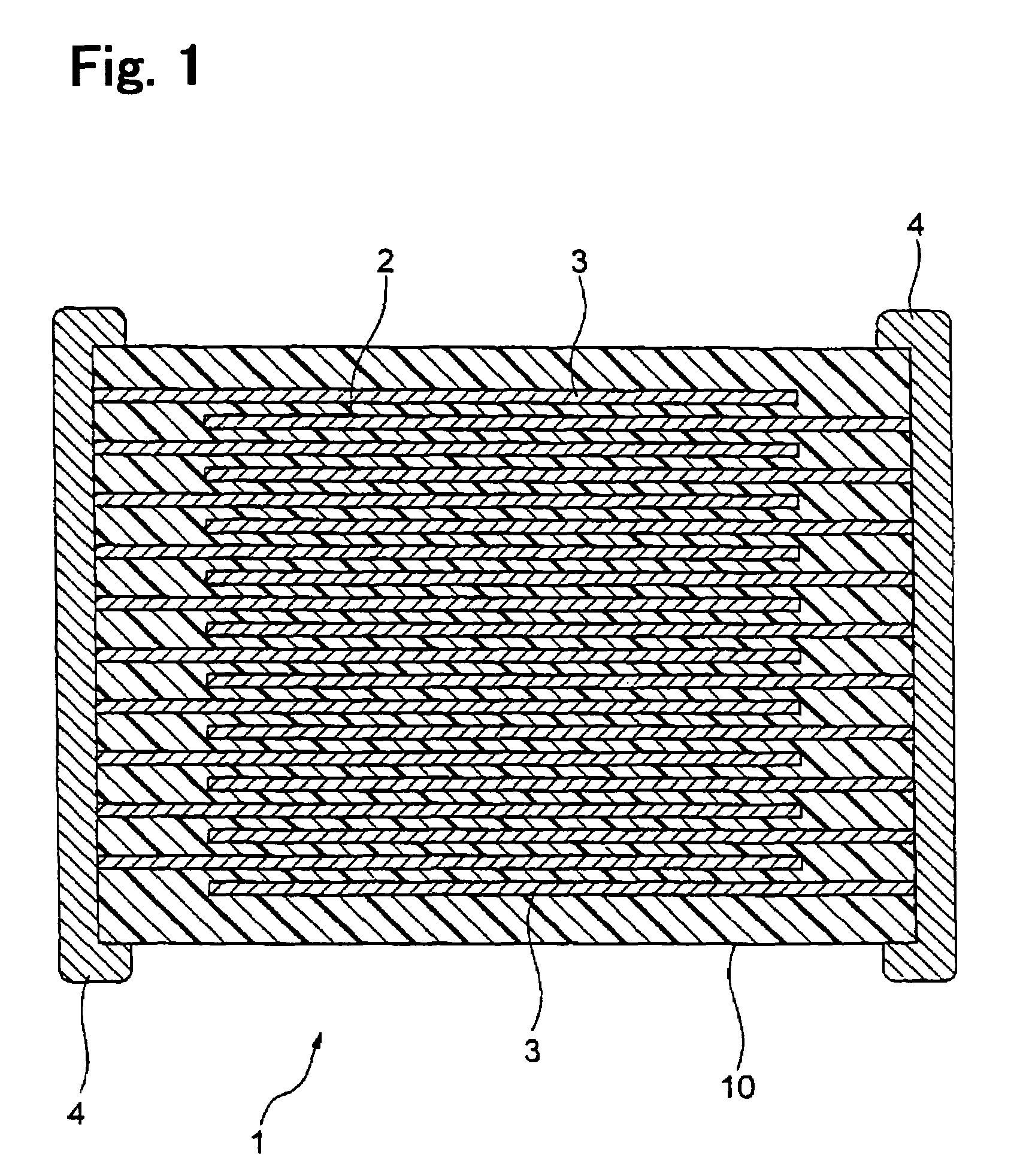
[0047]As shown in FIG. 1, a multilayer ceramic capacitor 1, one example of a multilayer ceramic electronic device of the present invention, has a capacitor device body 10 comprised of dielectric layers 2 and internal electrode layers 3 alternately stacked. This capacitor device body 10 is formed at its two ends with a pair of external electrodes 4 connected with the internal electrode layers 3 alternately arranged inside the device body 10. The internal electrode layers 3 are stacked so that the two end faces are alternately exposed at the surfaces of the two facing ends of the capacitor device body 10.

[0048]The pair of external electrodes 4 are formed at the two ends of the capacitor device body 10 and are connected to the exposed end faces of the alternately arranged internal electrode layers 3 to form a capacitor circuit.

[0049]The capacitor device body 10 is not particularly limited in outside shape or dimensions. These can be s...

second embodiment

[0088]The second embodiment is a modification of the above first embodiment. Only the material of the dielectric layers 2 differs. The rest of the configuration and the actions and effects are similar to the first embodiment. Below, only the different parts will be explained. Explanations of the common parts will be omitted.

[0089]In the present embodiment, the dielectric layers 2 include barium calcium titanate expressed by Ba1-xCaxTiO3 (0.001≦x≦0.15), a glass ingredient, and a sub ingredient. Barium calcium titanate is a compound comprised of barium titanate expressed by the formula (BaO)mTiO2 wherein part of the Ba of the A-site forming parts is substituted by Ca. If the value of x in the barium calcium titanate is too small, the temperature characteristic tends to deteriorate, while if too large, the dielectric constant tends to decline.

[0090]The glass ingredient in the present embodiment is not particularly limited. An alkali earth metal oxide, a mixture of Li2O3, B2O3, and SiO2...

example 1

Preparation of Dielectric Material

[0104]First, the barium titanate material, glass ingredient material, and sub ingredient material were prepared. As the barium titanate material, (BaO)m.TiO2 (where, m=1.005) one having a specific surface area (SSA) of 6 m2 / g was used. The barium titanate material was produced by preparing 1.000 mol of TiO2 with respect to 1.005 mol of BaCO3, wet mixing these by a ball mill for 16 hours, drying the mixture, then firing it at 800° C. in the air, then further wet pulverizing it by a ball mill for 100 hours. Note that the SSA is a value measured by the nitrogen absorption method, while m is found by the glass bead method.

[0105]As the glass ingredient material, a complex oxide constituted by (Ba0.6Ca0.4)SiO3 (below, called “BCG”) obtained by wet mixing BaCO3, CaCO3, and SiO2 in a predetermined ratio by a ball mill for 16 hours, drying the mixture, then firing it at 1150° C. in the air and further wet pulverizing the result by a ball mill for 100 hours i...


PUM

PropertyMeasurementUnit
thicknessaaaaaaaaaa
thicknessaaaaaaaaaa
thicknessaaaaaaaaaa

Abstract

A multilayer ceramic capacitor 1 having dielectric layers 2 having barium titanate or barium calcium titanate as a main ingredient. When the dielectric layers are barium titanate, the ratio of the grains having a thickness of the crystal grain boundaries 22 present between adjoining dielectric grains 20 is 30% to 95% of the plurality of dielectric grains 20 forming the dielectric layers 2. When the dielectric layers 2 are barium calcium titanate, the ratio of the grains having a thickness of the crystal grain boundaries 22 present between adjoining dielectric grains 20 is 20% to 70% of the plurality of dielectric grains 20 forming the dielectric layers 2.

Description

BACKGROUND OF THE INVENTION[0001]1. Field of the Invention[0002]The present invention relates to a multilayer ceramic capacitor or other electronic device, more particularly relates to a small-sized, large capacity electronic device superior in dielectric constant and other electrical characteristics, superior in temperature characteristic even when the dielectric layers are made thin, and high in reliability.[0003]2. Description of the Related Art[0004]In recent years, electrical products have been made increasingly smaller in size and higher in performance. Along with this, electronic devices are also being asked to be made smaller in size and higher in performance. In the case of an electronic device constituted as a multilayer ceramic capacitor, in particular a high capacity and high reliability are being sought.[0005]However, to obtain a small sized, high capacity multilayer ceramic capacitor, the dielectric ceramic layers and internal electrode layers have to be made thin. Alo...

Claims


Application Information

Patent Timeline
Patent Type & Authority Patents(United States)
IPC IPC(8): C04B35/468H01G4/06
CPCB82Y30/00C04B35/4682C04B35/6262C04B35/6264C04B35/64H01G4/1227H01G4/30C04B2235/3203C04B2235/3206C04B2235/3208C04B2235/3215C04B2235/3224C04B2235/3225C04B2235/3239C04B2235/3241C04B2235/3251C04B2235/3256C04B2235/3262C04B2235/3409C04B2235/3418C04B2235/3436C04B2235/3454C04B2235/36C04B2235/5409C04B2235/5445C04B2235/5454C04B2235/6025C04B2235/656C04B2235/6582C04B2235/6588C04B2235/663C04B2235/785C04B2235/79C04B2235/85H01G4/10H01G4/018H01G4/12
Inventor UMEDA, YUJIUEDA, SATOKOFUJIKAWA, YOSHINORISATO, AKIRA
Owner TDK CORPARATION
Why Eureka
Try Eureka