Light-emitting diode device and production method thereof

a technology of light-emitting diodes and production methods, which is applied in the direction of semiconductor devices, basic electric elements, electrical appliances, etc., can solve the problems of poor electron confinement, lowering the emission light output, and reducing the efficiency of hole injection, so as to enhance the crystallinity of a window layer and enhance the precision

Inactive Publication Date: 2009-05-05
RESONAC HOLDINGS CORPORATION
View PDF44 Cites 8 Cited by
  • Summary
  • Abstract
  • Description
  • Claims
  • Application Information

AI Technical Summary

Benefits of technology

[0026]To obtain a light-emitting diode device with enhanced precision that enhances crystallinity of a window layer and prevents generation of faults caused by a high-temperature process, a light-emitting diode device of the present invention comprises an AlGaInP active layer, a positive-electrode-side cladding layer and a negative-electrode-side cladding layer which sandwich the active layer and have an energy band gap value greater than an energy band gap value of the active layer, and a window layer which is formed on the positive-electrode-side cladding layer and has an energy band gap value greater than that of the active layer, wherein the positive-electrode-side cladding layer comprises an undoped AlInP layer grown to have a thickness of 0.5 μm or more and kept in contact with the active layer, and an intermediate layer doped to assume p-type conductivity, kept in contact with the window layer and having an intermediate energy band gap value between an energy band gap value of the undoped AlInP layer and that of the window layer.
[0032]Furthermore, in order to obtain a light-emitting diode device exhibiting good ohmic contact between an electrode and a semiconductor layer and high emission efficiency, a light-emitting diode device of the present invention comprises a semiconductor substrate having on its rear surface a first electrode, a semiconductor layer formed on the semiconductor substrate and including a light-emitting section formed of AlInGaP and a window layer formed atop the light-emitting section, a distribution electrode formed to extend along a portion of a surface of the window layer and kept in ohmic contact with the window layer, a transparent, electrically conductive film formed to cover the surface of the window layer and the distribution electrode and establishing electrical conduction with the distribution electrode, and a pad electrode formed on a portion of a surface of the transparent, electrically conductive film and establishing electrical conduction with the electrically conductive film.
[0041]The present invention further provides a light-emitting diode device with enhanced precision that enhances crystallinity of a window layer, prevents generation of faults and has a distribution electrode provided in the window layer.
[0042]In the DH-structure light-emitting diode device of the present invention having an AlGaInP active layer, as described above, the positive-electrode-side cladding layer comprises an undoped AlInP layer grown to have a thickness of 0.5 μm or more and in contact with the active layer, and an intermediate layer doped to assume p-type conductivity, in contact with the window layer and having an intermediate energy band gap value falling between the energy band gap value of the undoped AlInP layer and that of the window layer. Thus, the crystallinity of the window layer can be improved, and the luminance can be approximately doubled.

Problems solved by technology

Thus, the potential barrier increases upon injection of holes into the active layer, thereby decreasing the hole-injection efficiency.
In addition, the barrier level of the cladding layer with respect to the electrons confined in the active layer decreases, leading to poor electron confinement.
As a result, occurrence of recombination of electrons and holes becomes less frequent, thereby lowering emission light output.
However, when the window layer has a large resistivity, the voltage required for supplying rating current to the LED device increases.
Thus, problems occur in a portion of the device other than the window layer, resulting in a failure to produce an LED device of high output intensity.
However, in the aforementioned conventional light-emitting device, sufficient ohmic contact between the transparent, electrically conductive film and the surface of the light-emitting section fails to be attained, leading to an increase in forward voltage and deterioration of lifetime characteristics.
In the light-emitting device disclosed in JP-A HEI 11-17220, although ohmic contact between the transparent, electrically conductive film and the semiconductor layer is improved, emitted light is absorbed in the contact layer provided on the light-emitting section, and therefore, high-luminance emission fails to be obtained, and emission efficiency is not improved.
This interception has been found to be a cause of lowering of emission efficiency.

Method used


Image

  • Light-emitting diode device and production method thereof
  • Light-emitting diode device and production method thereof
  • Light-emitting diode device and production method thereof

Examples


Embodiment Construction

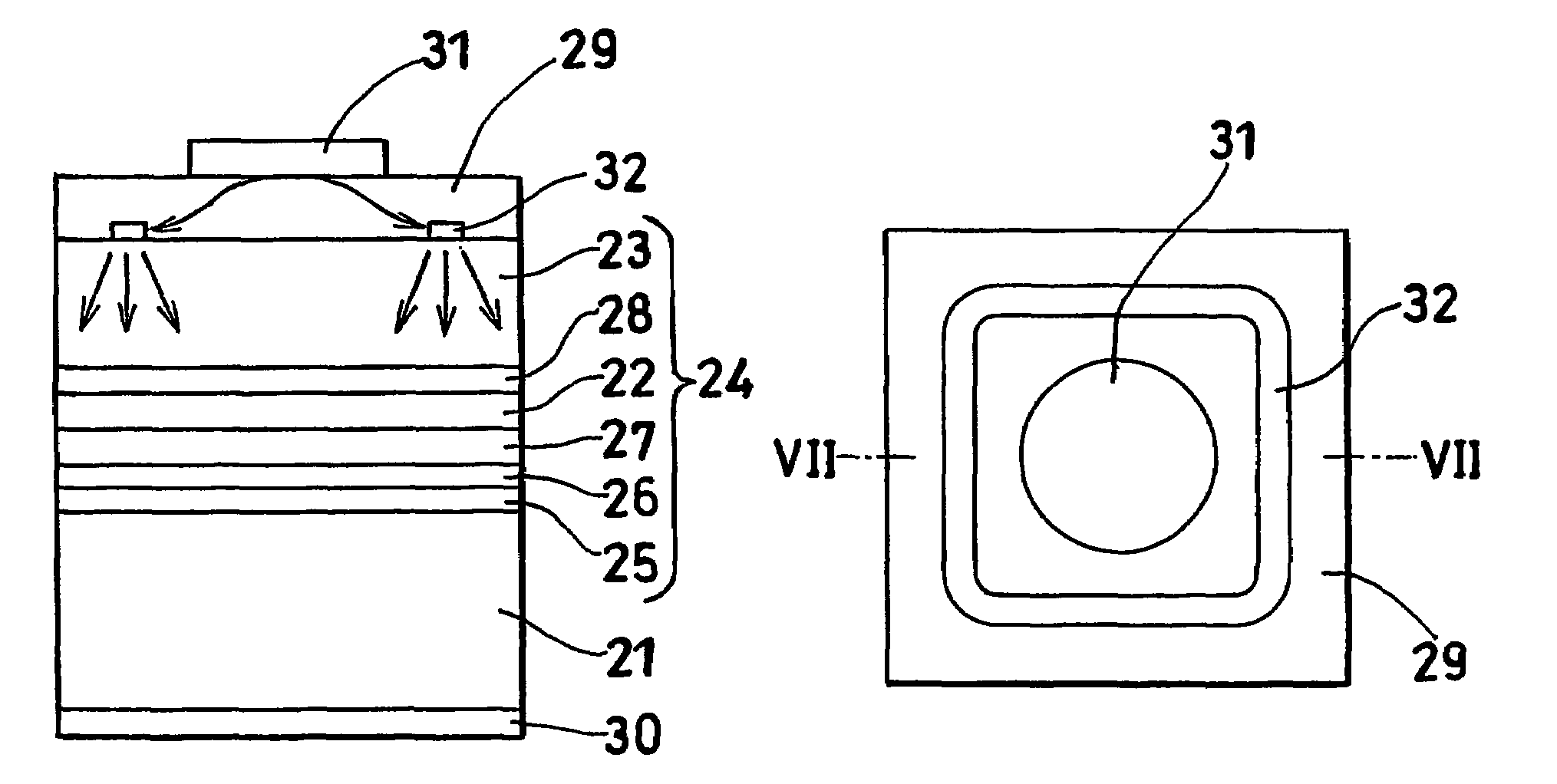
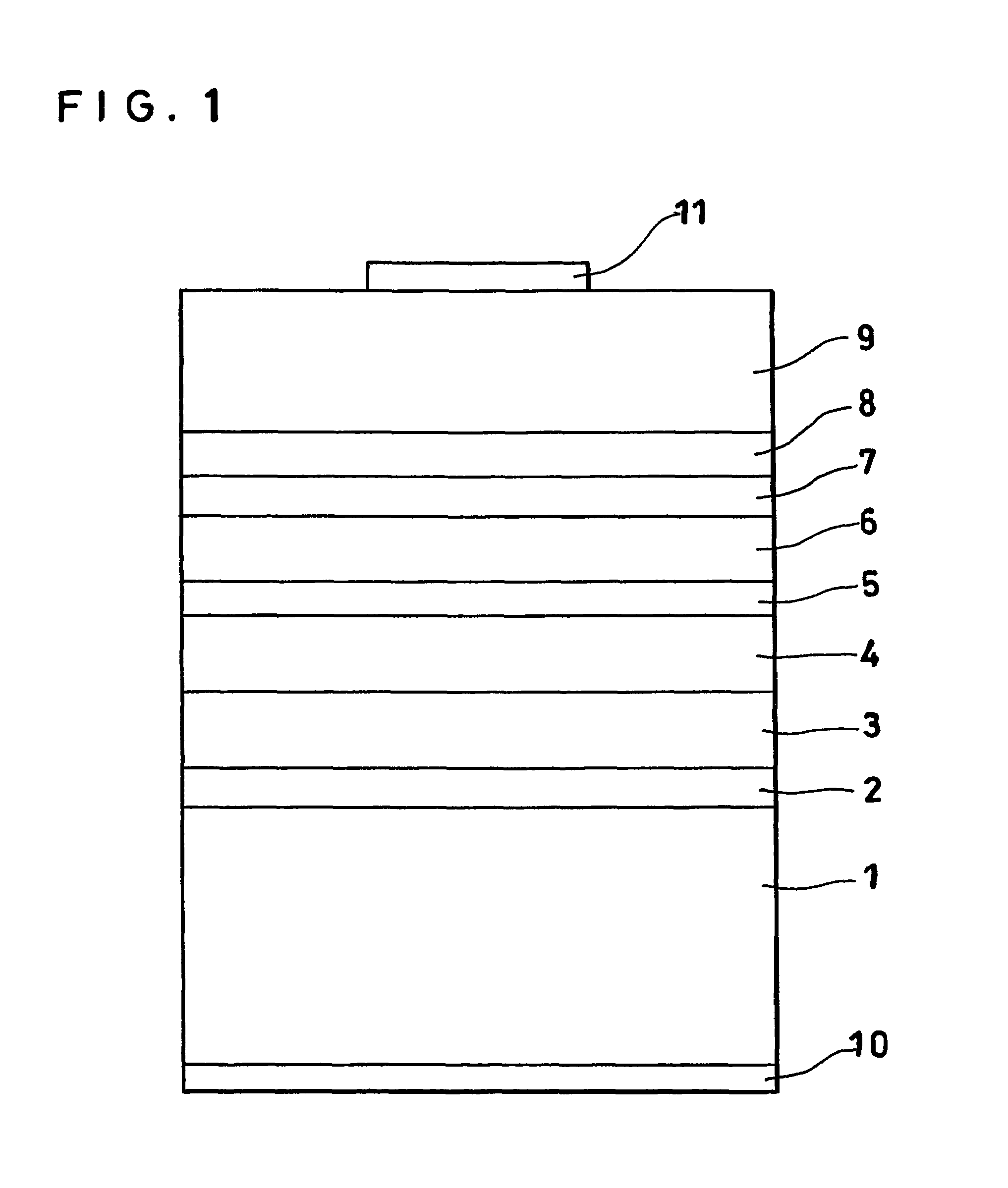
[0067]FIG. 1 is a schematic cross section showing one embodiment of a double hetero structure light-emitting diode (LED) device having an AlGaInP active layer according to the present invention. In this embodiment, on a substrate 1 there are formed a buffer layer 2, a reflection layer 3, an n-type cladding layer 4, a first undoped AlInP layer 5, an active layer 6, a second undoped AlInP layer 7, a p-type intermediate layer 8 and a window layer 9 in this order, with an n-electrode 10 provided on the backside of the substrate 1 and with a p-electrode 11 provided on the front surface of the window layer 9.

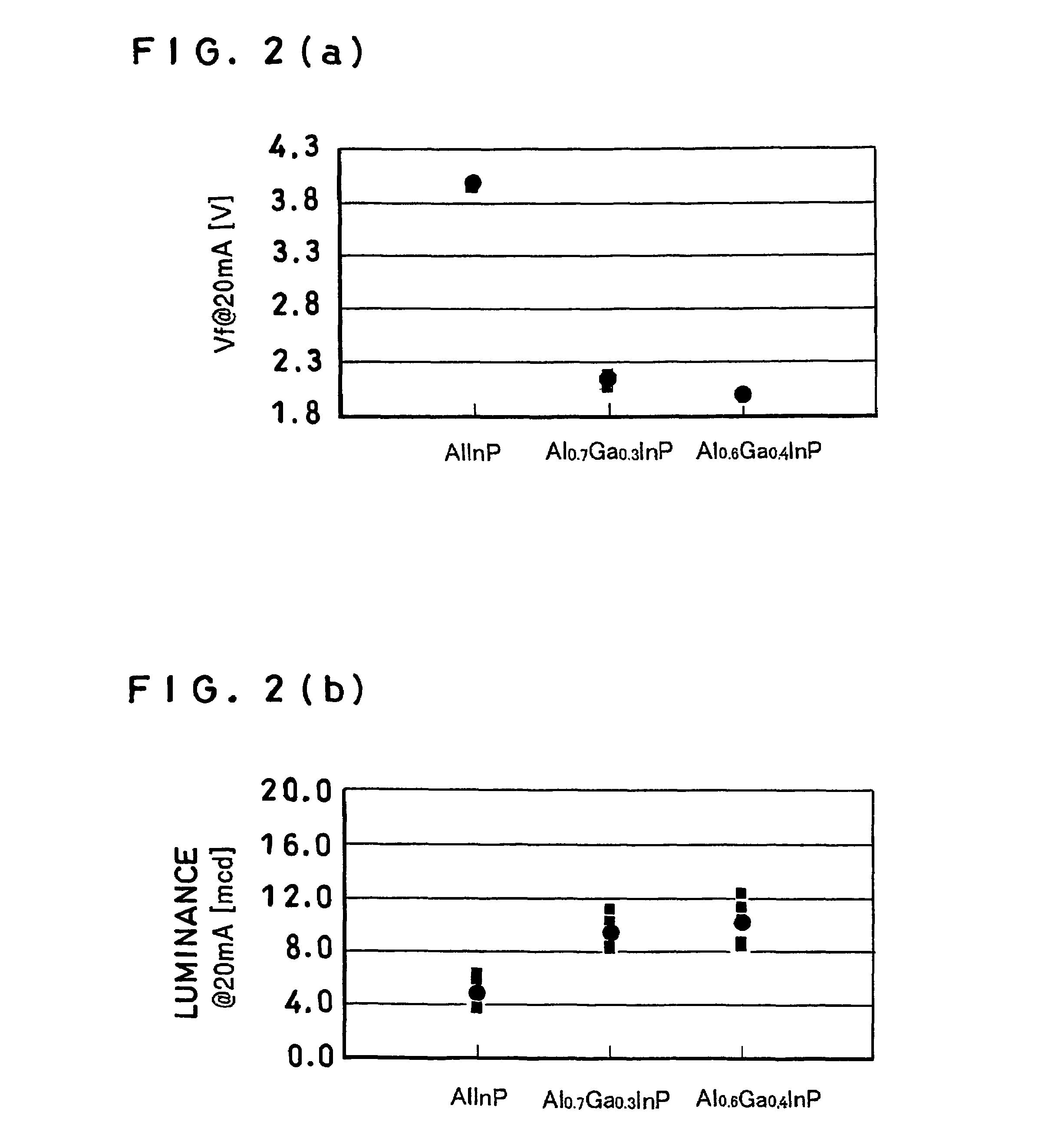
[0068]The substrate 1 used in this embodiment is a silicon (Si)-doped gallium arsenide (GaAs) substrate (15°-off relative to (100)). On the substrate, the layers listed in Table 1 below are formed by use of trimethylgallium (Ga (CH3)3), trimethylindium (In(CH3)3), trimethylaluminum (Al(CH3)3), dimethylzinc (Zn(CH3)2), disilane (Si2H6), arsine (AsH3) and phosphine (PH3). Notably, durin...


PUM


Abstract

A double hetero structure light-emitting diode device includes an active layer (6), a positive-electrode-side cladding layer, a negative-electrode-side cladding layer (4), a window layer (9) and an undoped AlInP layer. The positive-electrode-side cladding layer includes an undoped AlInP layer (7) grown to have a thickness of 0.5 μm and an intermediate layer (8) doped to assume p-type conductivity and having an intermediate energy band gap value between that of the undoped AlInP layer and that of the window layer. The window layer on the intermediate layer is a GaP layer grown at 730° C. or higher and at a growth rate of 7.8 μm / hour or more in the presence of Ze serving as a dopant. The negative-electrode-side cladding layer is provided with an undoped AlInP layer (5) having a thickness of 0.1 μm or more. With this configuration, there is provided a light-emitting diode device that enhances the crystallinity of a window layer, prevents generation of faults caused by a high-temperature process and attains high luminance at a wavelength falling within a yellow-green band.

Description

CROSS REFERENCE TO RELATED APPLICATIONS[0001]This application is an application filed under 35 U.S.C. §111(a) claiming the benefit pursuant to 35 U.S.C. §119(e)(1) of the filing dates of Provisional Application Ser. No. 60 / 448,104 filed Feb. 20, 2003 and Provisional Application Ser. No. 60 / 456,561 filed Mar. 24, 2003 pursuant to 35 U.S.C. §111(b).TECHNICAL FIELD[0002]The present invention relates to a light-emitting diode (LED) device emitting visible light and to a method for producing the LED deviceBACKGROUND ART[0003]LEDs find a variety of uses including display devices. As is well known, the emission wavelength of LEDs employing a semiconductor depends on the type of the semiconductor and increases in the order of InGaN, AlGaInP, GaAlAs and GaInAsP. Year by year, the luminance of LEDs has been improved, and a high-luminance LED is now employed as an illuminator or a backlight of liquid crystal display devices. However, studies on further improvement of the luminance are underway...

Claims


Application Information

Patent Timeline
Patent Type & Authority Patents(United States)
IPC IPC(8): H01L21/00H01L33/02H01L33/14H01L33/30
CPCH01L33/30H01L33/14H01L33/02
Inventor TAKEUCHI, RYOUICHIMATSUZAWA, KEIICHIYAMAZAKI, JUNICHI
Owner RESONAC HOLDINGS CORPORATION
Why Eureka
Try Eureka