
Eureka
For R&D, Eureka makes reading and utilizing patents & technical documents easy.
Eureka AIR
Designed for self-driven R&D workflows. Generate viable solutions, solve complex R&D challenges, empower your innovation with AI.

Eureka Materials
Designed for material experts only. Revolutionize your material R&D, from search, analyze, to developing new materials.

TechResearch
Generate reliable direction feasibility study reports for your R&D in just a few steps.

TechSeek
Discover and master advanced knowledge NOW. Basics, ideas, possibilities, all at once.

TechMind
As an expert in R&D Theories, TechMind can generates customized viable solutions instantly.

TechRisk
Analyze your overall solution with one click, know your potential R&D risks in advance.

TechMonitor
Get weekly tech updates, stay abreast of the latest tech innovations and key insights.
Display element
- Summary
- Abstract
- Description
- Claims
- Application Information
AI Technical Summary
Benefits of technology
Problems solved by technology
Method used
Image

Examples
example 1
Reflection Type Display Element
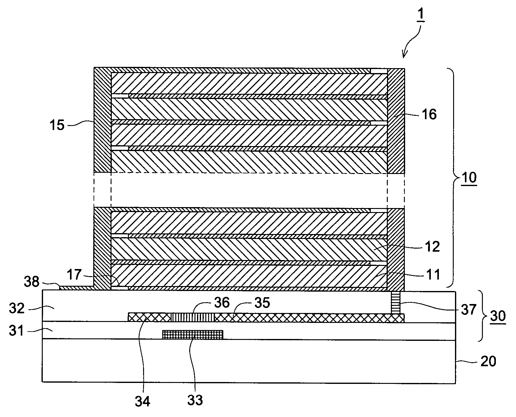
[0076]In the structure shown in FIG. 2, a reflection type display element was manufactured and color display was performed by application of electric field. This example will be explained below. Reference will be made to FIGS. 2 and 3 wherever required.
[0077]The following describes the conditions wherein the organic TFT element was formed on the substrate.
[0078]A glass substrate with an ITO film formed on the surface to a thickness of 125 nm was used as a substrate. The glass substrate had a dimension of 200 mm×200 mm. A resist is formed on this substrate to a thickness of about 1 μm. First, the gate electrode and gate bus were provided through the processes of exposure, development and etching of an ITO film and separation of the resist. The photomask used in this process has the pattern to arrange a total of 100 TFTs (10×10) on the substrate.
[0079]Second, a 500 nm SiO2 film was formed as a gate insulating film by the plasma CVD (chemical vapor deposi...
example 2
Transparent Type Display Element
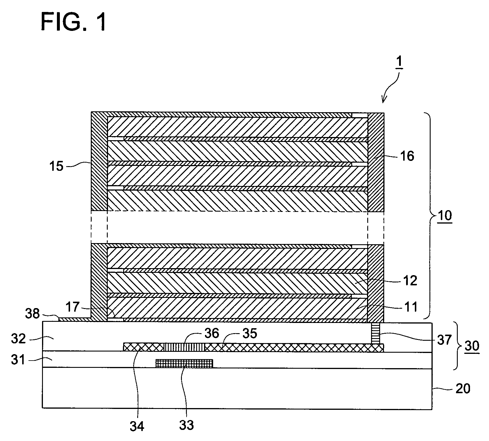
[0096]A transparent type display element was manufactured using the structure shown in FIG. 2. The following describes an example of color display through application of electric field with reference to FIG. 2 wherever required.
[0097]The conditions for forming an organic TFT element on the substrate were the same as those wherein the reflection type display element was formed. However, the second electrode on the top surface of the passivation layer was formed by dropping PEDOT:PSS. In the reflection type display element, the second electrode was formed of carbon black, and was used also as a light absorbing layer. In the transparent type display element, the second electrode was required to be a transparent conductive film.
[0098]The conditions for forming a layered body (actuator) were the same as those wherein the reflection type display element was formed. The description will be omitted to avoid duplication.
[0099]An electric field was applied to t...
example 3
Pattern for Clock Display
[0103]The structure of the layered body is the same as that of the aforementioned display element. The following describes an example showing manufacturing a display element having a clock display pattern based on seven display sections 61 shown in FIGS. 6(a) and 6(b), and its color display by application of an electric field. Reference will be made to FIG. 2 and FIGS. 6(a) and 6(b) as required.
[0104]FIG. 6(a) is a drawing showing the arrangement pattern of the display element and FIG. 6(b) is a cross sectional view taken along line AA′.
[0105]To manufacture the substrate, a drive electrode 62 was patterned on the glass substrate 20 equipped with a ITO (indium tin oxide). The drive electrode 62 is connected to the power source (not illustrated).
[0106]A passivation layer 67 was further formed on the substrate by coating an aqueous solution containing PVA coated by spin coating. After that, contact hole 63 was formed by laser. This allows the drive electrode 62...
PUM
 Abstract
Description
Claims
Application Information
 - R&D Engineer
- R&D Manager
- IP Professional
- Industry Leading Data Capabilities
- Powerful AI technology
- Patent DNA Extraction
Browse by: Latest US Patents, China's latest patents, Technical Efficacy Thesaurus, Application Domain, Technology Topic, Popular Technical Reports.
© 2024 PatSnap. All rights reserved.Legal|Privacy policy|Modern Slavery Act Transparency Statement|Sitemap|About US| Contact US: help@patsnap.com