Surface and composition enhancements to high aspect ratio C-MEMS

a technology of c-mems and surface enhancement, applied in the field of carbon microelectromechanical systems, can solve the problems of poor repeatability of carbon composition, low feature resolution, time-consuming and expensive, etc., and achieve high aspect ratio and/or nanoscale surface enhancement, high surface area, and improved system and method for producing such structures

Active Publication Date: 2009-05-19
RGT UNIV OF CALIFORNIA
View PDF12 Cites 12 Cited by
  • Summary
  • Abstract
  • Description
  • Claims
  • Application Information

AI Technical Summary

Benefits of technology

[0007]The present invention provides an improved C-MEMS architecture having carbon structures with high aspect ratios and / or nanoscale surface enhancements, and improved systems and methods for producing such structures. In many applications where carbon micro-structures act as a transfer interface (e.g. electrodes for battery applications, graft sites for DNA immobilization, sensing electrodes for chemical sensors, etc.), high surface area is desirable. The high aspect ratios and nanoscale surface enhancements provided herein advantageously significantly increase the surface area of the carbon micro-structures.
[0008]In one embodiment, which is described below as an example only and not to limit the invention, the surface of carbon micro-structures is nanotextured to increase the surface area of the carbon micro-structures. Nanotexturing of the surface of the carbon micro-strutures can be accomplished through oxygen plasma exposure of the carbon micro-structures or carbon precursor polymer micro-structures prior to pyrolysis. The plasma roughens the surface of the microstructure, creating a pumice-like nanotextured surface.
[0009]In another embodiment, which is described below as an example only and not to limit the invention, carbon micro-structures can be covered with a rich coat of nanoscale structures such as nanotubes, nanowires, nanofibers and the like, that hugely increases the surface area of the micro-structures. For example, for Li ion microbattery application, integration of carbon nanotubes and Si nanowires on the C-MEMS electrodes will increase the electrode surface areas and, thus, the Li storage capacity and power density, and decrease battery charge / discharge rates.

Problems solved by technology

Yet, microfabrication of C-MEMS carbon structures using current processing technology, including focus ion beam (FIB) and reactive ion etching (RIE), tends to be time consuming and expensive.
Low feature resolution, and poor repeatability of the carbon composition as well as the widely varying properties of the resulting devices limits the application of screen printing of commercial carbon inks for C-MEMS.
The fabrication of high aspect ratio and dense C-MEMS patterns is a challenging problem because with increasing photoresist thickness, the requirements of any lithography process increase exponentially.
Basically, it is very difficult to design a thick positive tone photoresist chemistry to achieve the necessary transparency and to achieve reasonable exposure doses while maintaining excellent sidewall angles.
However, this technique requires an expensive synchrotron source, hence the motivation for cheaper and easier processes.

Method used


Image

  • Surface and composition enhancements to high aspect ratio C-MEMS
  • Surface and composition enhancements to high aspect ratio C-MEMS
  • Surface and composition enhancements to high aspect ratio C-MEMS

Examples


Embodiment Construction

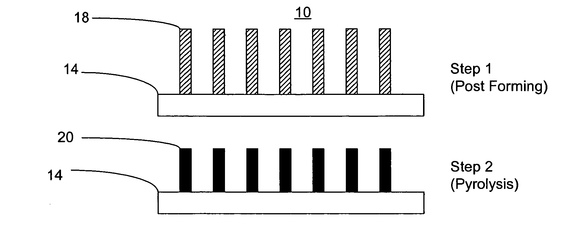
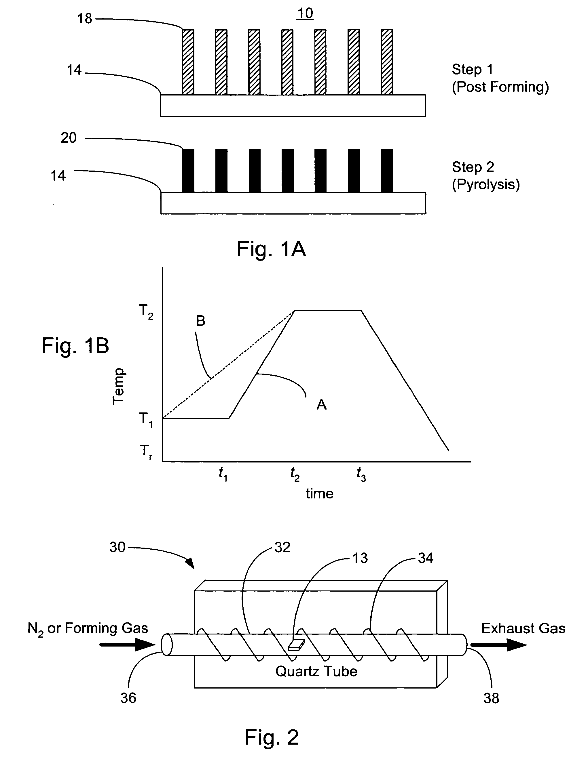
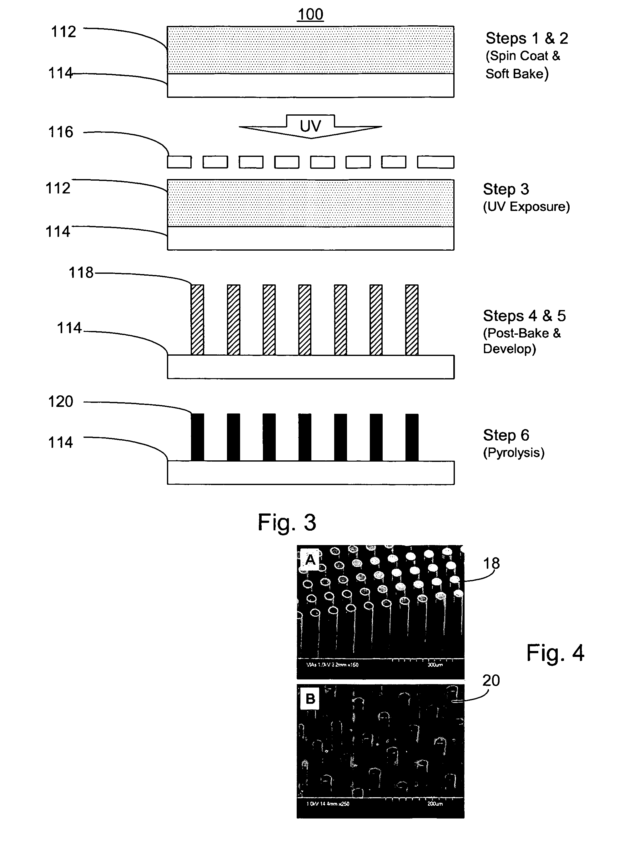
[0034]Referring in detail to the figures, the systems and methods described herein facilitate the production of high aspect ratio carbon-micro-electro-mechanical systems (C-MEMS) structures, as well as C-MEMS structures with nanoscale surface enhancements thereto. In one embodiment, as depicted in FIGS. 1A and 1B, high aspect ratio carbon posts, having aspect ratios greater than 10:1, are microfabricated by pyrolyzing polymer posts patterned from a carbon precursor polymer. In step 1 of the process 10, polymer posts 18 are patterned or formed in an array on a substrate 14. The posts 18 can be formed by a variety of processes including, but not limited to, photolithography, soft lithography methods including stamping or micro contact printing, hot embossing or nanoimprinting, step and flash lithography, micro injection molding and the like, silk screening, spray deposition techniques including plasma spraying and the like, self-assembly of malleable polymers and liquids using electri...


PUM

PropertyMeasurementUnit
thickaaaaaaaaaa
diameteraaaaaaaaaa
thicknessaaaaaaaaaa

Abstract

C-MEMS architecture having carbon structures with high surface areas due to high aspect ratios and nanoscale surface enhancements, and improved systems and methods for producing such structures are provided. Specifically, high aspect ratio carbon structures are microfabricated by pyrolyzing a patterned carbon precursor polymer. Pyrolysing the polymer preferably comprises a multi-step process in an atmosphere of inert and forming gas at high temperatures that trail the glass transition temperature (Tg) for the polymer. The surface area of the carbon microstructures is increases by nanotexturing the surface through oxygen plasma exposure, and by integrating nanoscale structures with the carbon microstructures by exposing the carbon microstructures and a catalyst to hydrocarbon gas. In a preferred embodiment, the carbon microstructures are the source of carbon gas.

Description

CROSS-REFERENCE TO RELATED APPLICATIONS[0001]This application claims the benefit of U.S. Provisional Application Nos. 60 / 615,311 filed Sep. 30, 2004, and 60 / 615,088 filed Oct. 1, 2004, which are fully incorporated by reference herein.FIELD OF THE INVENTION[0002]The present invention relates to carbon micro-structures and, more particularly, to carbon micro-electro-mechanical-systems (C-MEMS) having carbon structures with high surface areas due to high aspect ratios and surface enhancements, and systems and methods for producing such structures.BACKGROUND OF THE INVENTION[0003]Recent attention has focused on carbon micro-electro-mechanical-systems (C-MEMS). Yet, microfabrication of C-MEMS carbon structures using current processing technology, including focus ion beam (FIB) and reactive ion etching (RIE), tends to be time consuming and expensive. Low feature resolution, and poor repeatability of the carbon composition as well as the widely varying properties of the resulting devices l...

Claims


Application Information

Patent Timeline
Patent Type & Authority Patents(United States)
IPC IPC(8): C23C6/00
CPCB81C1/00111B81C1/00547B82Y30/00C23C16/04C23C16/26Y10S977/844Y10S977/947
Inventor MADOU, MARC J.WANG, CHUNLEITAHERABADI, LILIPARK, BENJAMINZAOUK, RABIH
Owner RGT UNIV OF CALIFORNIA
Why Eureka
Try Eureka