Semiconductor device with a cooling element

Inactive Publication Date: 2009-07-28
OSRAM GMBH
View PDF22 Cites 4 Cited by
  • Summary
  • Abstract
  • Description
  • Claims
  • Application Information

AI Technical Summary

Benefits of technology

[0007]The object underlying the present invention is, in a device of the species cited at the beginning hereof, to improve the thermal and mechanical coupling of the semiconductor component to the microcooler. The invention is particularly intended to provide both high heat dissipation efficiency and high mechanical stability of the arrangement.
[0013]The invention is therefore based on the idea of conducting the heat from the semiconductor component to the coolant by the shortest possible path and simultaneously guaranteeing the mechanical stability of the connection between the semiconductor component and the cooling element by means of an intermediate support that compensates for differing expansions.
[0015]The intermediate support therefore equalizes the differential thermal expansion of the semiconductor component and the cooling element through completely reversible strain. Mechanical loading of the semiconductor component thus is largely prevented.
[0017]In a preferred embodiment of the invention, the semiconductor component is fastened to the intermediate support by means of a hard solder. Since according to the invention the intermediate support accommodates the differential thermal expansion, this function no longer has to be performed by a plastically deformable soft solder, as in the prior-art designs. This creates the freedom instead to use a high-temperature-resistant and cycle-stable hard solder to fasten together the component and the intermediate support.
[0021]In a preferred embodiment of the semiconductor device of the invention, it is provided that the intermediate support is made of molybdenum, tungsten, a copper / molybdenum alloy or a copper / tungsten alloy. The copper content of the copper / molybdenum or copper / tungsten alloy is advantageously between about 10% and about 20%. These materials have a high modulus of elasticity of more than 250 GPa or even in excess of 300 GPa. They further offer a high yield stress and high temperature stability.

Problems solved by technology

A disadvantage with respect to heat transfer to the coolant is the fact that no microstructured area can be placed directly under the laser bar 12 because of the seal.
As a result of temperature-change loads of the kind that occur, for example, during cooling after the soldering step or when the laser bar is turned on and off, plastic deformation can occur in the soft solder—in the case of indium, for example, in response to temperature increases of as little as 5° C. to 7° C. This deformation can cause the connection to be partially or completely broken.
A partially or completely interrupted connection delivers much poorer heat dissipation and an undesirable inhomogeneous power distribution in the laser bar.

Method used


Image

  • Semiconductor device with a cooling element
  • Semiconductor device with a cooling element

Examples


Embodiment Construction

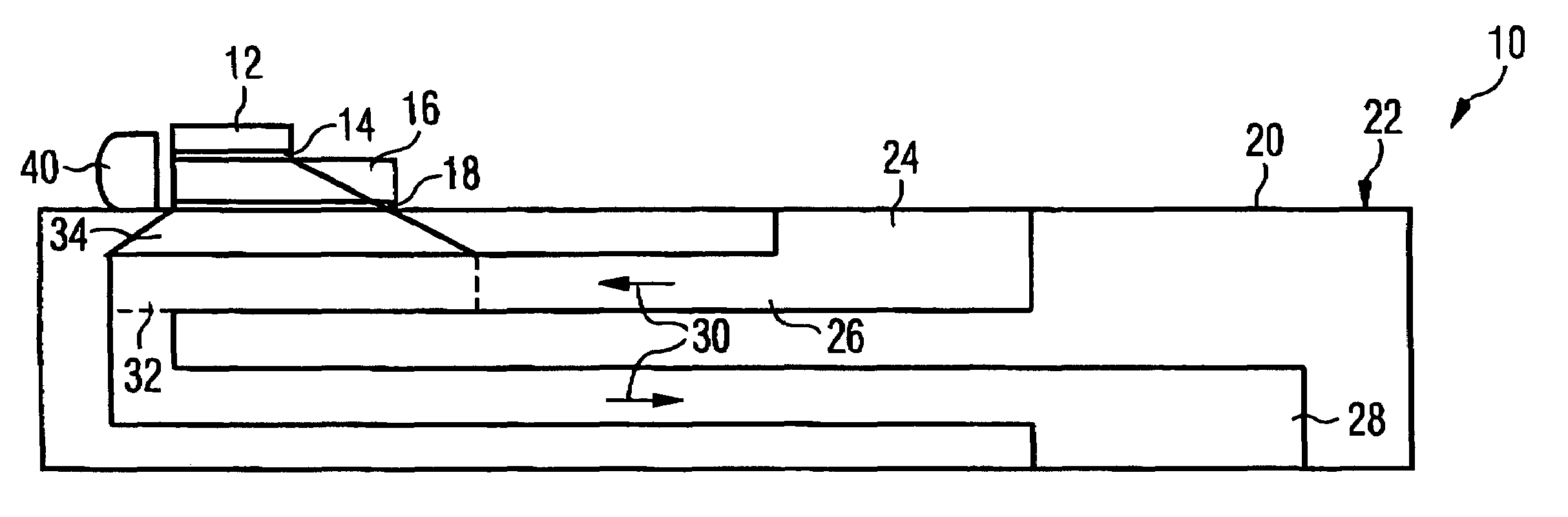
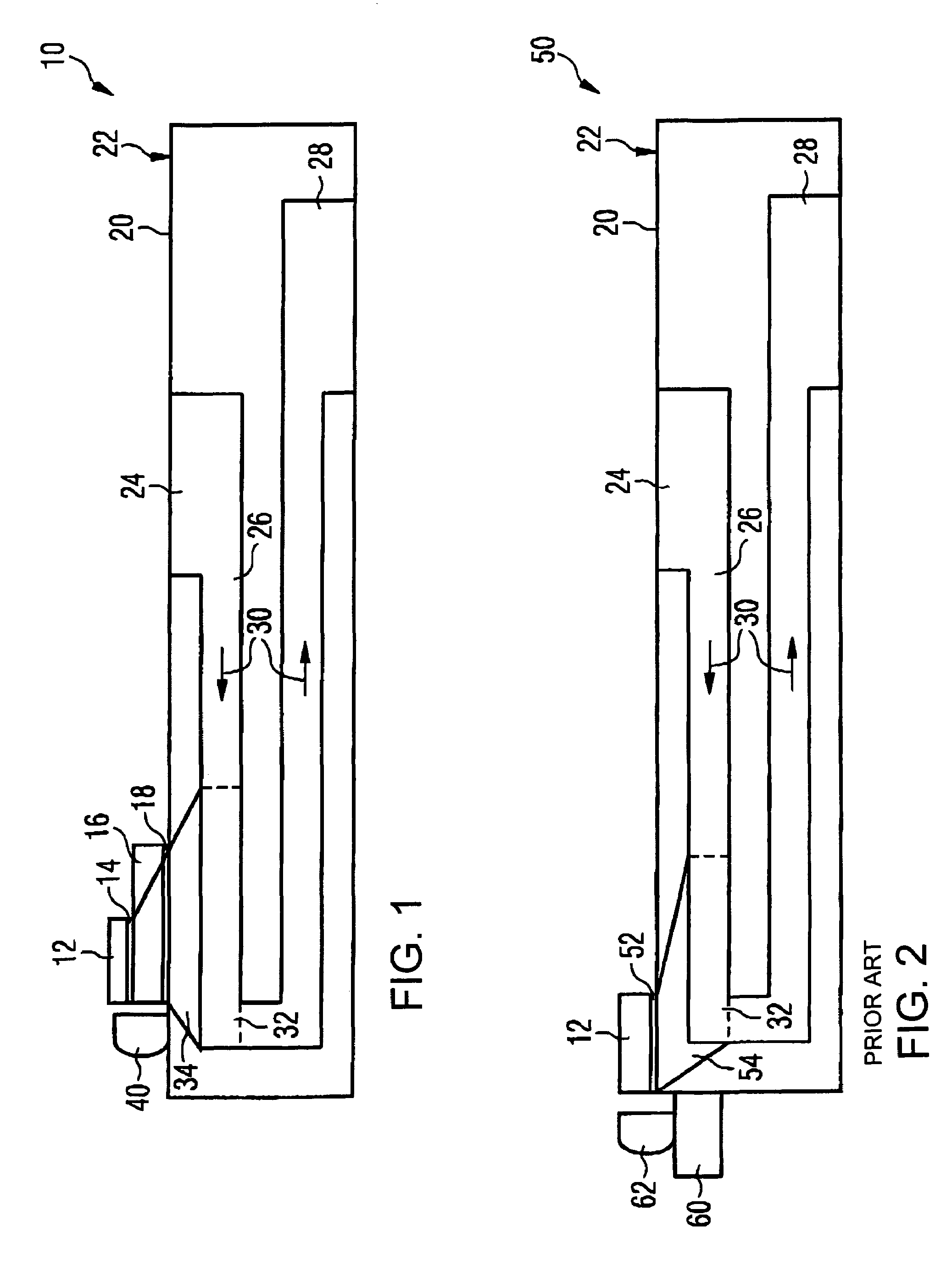
[0034]The semiconductor device 10 illustrated in section in FIG. 1 comprises a power laser diode bar 12, which is soldered onto a microooler 20 having a coolant inlet 24 on its upper face, a cooling channel 26 in its interior and a coolant outlet 28 on its bottom face. The direction of flow of the coolant in the microcooler 20 is indicated by arrows 30.

[0035]Cooling channel 26 comprises, in a region 32 beneath power laser diode bar 12, microstructures, for example a plurality of channels each measuring 0.3 mm in width and height. Such microstructures cause turbulence in the flowing coolant by means of which the exchange of heat between the coolant and the microcooler can be configured very effectively.

[0036]The length of the microstructured region 32 in cooling channel 26 is at least equal to the length of power laser diode bar 12, which completely overlaps microstructured region 32 at least in this direction of extent. Preferably, as illustrated in FIG. 1, the length of microstruct...


PUM


Abstract

A semiconductor device comprising a semiconductor component, particularly a power laser diode bar, disposed on a cooling element, wherein the cooling element contains in its interior a cooling channel for conducting a coolant. The coolant channel comprises in at least one region microstructures for effective heat transfer to the coolant. The semiconductor component substantially completely overlaps the region of the cooling channel comprising the microstructures. Disposed between the semiconductor component and the cooling element is an intermediate support so arranged and configured that it compensates for mechanical stresses between the semiconductor component and the cooling element occurring as a result of differing thermal expansions of the semiconductor component and the cooling element. The material of the cooling element particularly preferably has a high modulus of elasticity such that the compensation takes place substantially within the elastic strain regime.

Description

CROSS-REFERENCE TO RELATED APPLICATIONS[0001]This application is the National Stage of International Application No. PCT / DE2003 / 001906, filed Jun. 10, 2003, which claims the benefit of German Patent Application Ser. No. 10234704.2, filed on Jul. 30, 2002. The contents of both applications are hereby incorporated by reference in their entireties.FIELD OF THE INVENTION[0002]The invention concerns a semiconductor device comprising a semiconductor component, particularly a laser diode or a laser bar, disposed on a cooling element, wherein the cooling element contains in its interior a cooling channel serving to conduct a coolant and comprising in at least one region microstructures for effective heat transfer to the coolant.BACKGROUND OF THE INVENTION[0003]A known semiconductor device of this kind is depicted and described, for example, in patent DE 195 06 093 02. A schematic diagram of such a known semiconductor device is provided in FIG. 2. In that case, a microcooler 20 is fabricated...

Claims


Application Information

Patent Timeline
IPC IPC(8): H01S3/04H01S5/00H01S5/024H01L23/473H01S5/40
CPCH01L23/473H01S5/4025H01S5/02272H01S5/02423H01L2924/0002H01S5/02484H01L2924/00H01S5/0237
Inventor GROETSCH, STEFAN
Owner OSRAM GMBH
Why Eureka
Try Eureka