Spin transfer MRAM device with separated CPP assisted writing

a technology of assisted writing and transfer mram, which is applied in the direction of semiconductor devices, digital storage, instruments, etc., can solve the problems of destroying a thin tunnel barrier layer such as mgo, difficult to apply a sufficient electric current to the address wiring, and a large electric current magnetic field in the device, so as to increase the read and write efficiency

a technology of assisted writing and transfer mram, which is applied in the direction of semiconductor devices, digital storage, instruments, etc., can solve the problems of destroying a thin tunnel barrier layer such as mgo, difficult to apply a sufficient electric current to the address wiring, and a large electric current magnetic field in the device, so as to increase the read and write efficiency

US7577021B2Active Publication Date: 2009-08-18TAIWAN SEMICON MFG CO LTD

Image

  • Spin transfer MRAM device with separated CPP assisted writing
  • Spin transfer MRAM device with separated CPP assisted writing
  • Spin transfer MRAM device with separated CPP assisted writing

Examples


Embodiment Construction

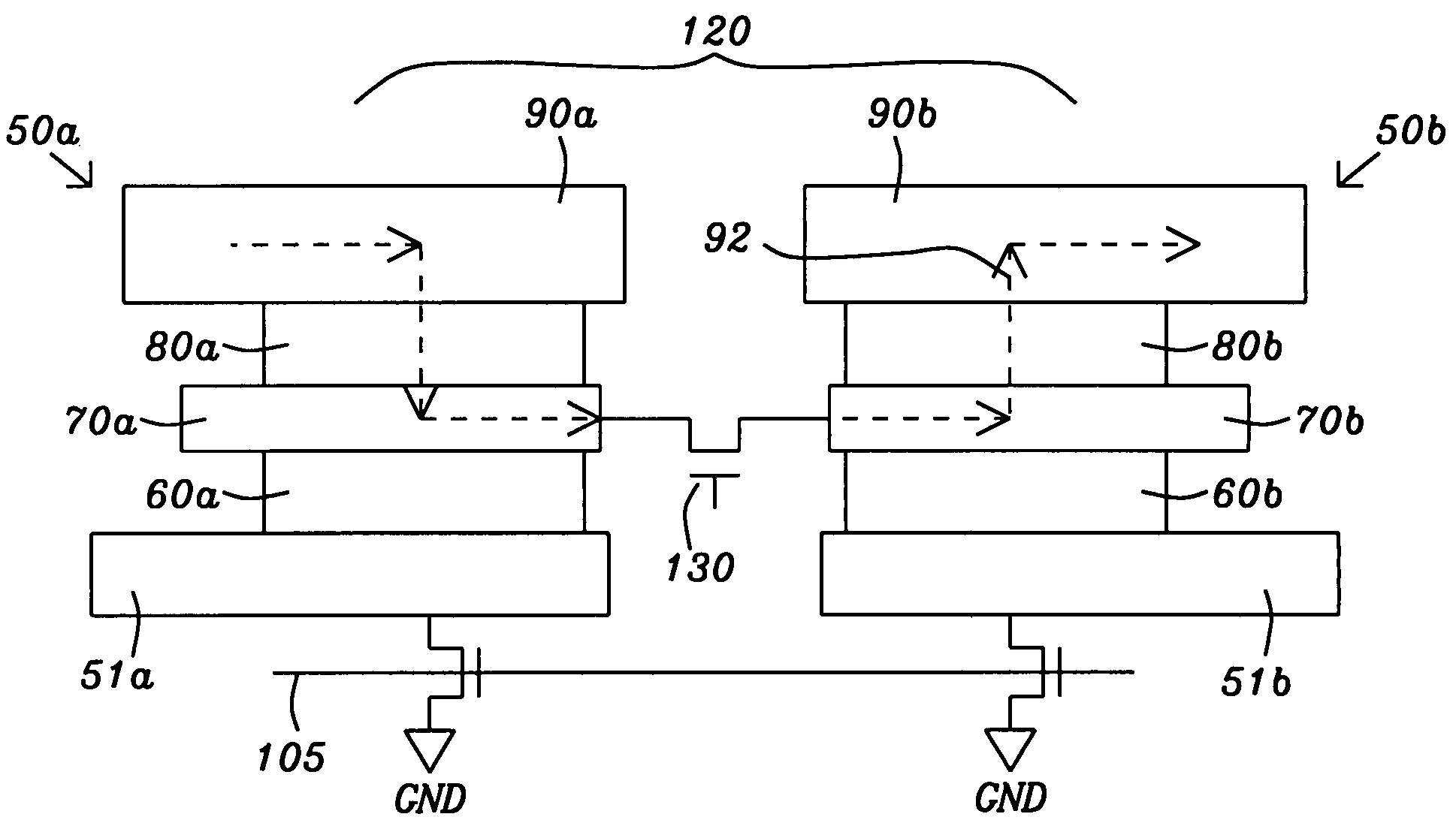
[0035]One aspect of the present invention is a CPP / MTJ sub-cell configuration within a Spin-RAM device that provides for a separation of write and read pathways so that the writing process and reading process can be independently optimized. In the CPP and MTJ cells, the exemplary embodiment depicts a single spin valve structure. However, the present invention also encompasses a CPP / MTJ sub-cell wherein one or both of the CPP cell and MTJ cell have a dual spin valve configuration. Devices based on this technology may be referred to as Spin-RAM or spin-transfer MRAM devices. Another aspect of the present invention is a wiring scheme comprised of a plurality of bit cells, word lines, and bit lines that takes advantage of a pair of CPP / MTJ sub-cells within each bit cell which enables the reading process to be more efficient. Those skilled in the art will appreciate that the terms “magnetic moment” and “magnetization direction” may be used interchangeably.

[0036]First, the CPP / MTJ sub-cel...


PUM


Abstract

A spin-transfer MRAM is described that has two sub-cells each having a conductive spacer between an upper CPP cell and a lower MTJ cell. The two conductive spacers in each bit cell are linked by a transistor which is controlled by a write word line. The two CPP cells in each bit cell have different resistance states and the MTJ cell and CPP cell in each sub-cell have different resistance states. The MTJ free layer rotates in response to switching in the CPP free layer because of a large demagnetization field exerted by the CPP free layer. An improved circuit design is disclosed that enables a faster and more reliable read process since the reference is a second MTJ within the same bit cell. When RMTJ1>RMTJ2, the bit cell has a "0" state, and when RMTJ1<RMTJ2, the bit cell has a "1" state.

Description

FIELD OF THE INVENTION[0001]The invention relates to a spin-transfer MRAM cell in which an upper CPP cell is separated from a lower MTJ cell by a conducting layer in order to form different read and write paths, and each bit cell has two spin-transfer MRAM cells that are written into opposite resistance states.BACKGROUND OF THE INVENTION[0002]Magnetoresistive Random Access Memory (MRAM), based on the integration of silicon CMOS with magnetic tunnel junction (MTJ) technology, is a strong candidate to provide a dense (8-25F2 cell size), fast (1˜30 ns read / write speed), and non-volatile storage solution for future memory applications. The MTJ utilizes a thin dielectric insulating layer like AlOx, AlNxOy, or MgOx that is formed between a first ferromagnetic layer which is pinned in a certain direction by an adjacent anti-ferromagnetic (AFM) layer, and a second ferromagnetic (free) layer. The pinned layer has a magnetic moment that is fixed in the “y” direction, for example, by exchange ...

Claims


Application Information

Patent Timeline
18 Aug 2009
Publication
US7577021B2
IPC
G11C11/00
CPC
G11C11/16; H01L27/226; Y10S977/935; G11C11/1659; G11C11/161; G11C11/1673; G11C11/1675; G11C11/1657
Inventors
GUO, YIMIN; CHIEN, JEFF