Method of fabricating a semiconductor device using plasma to form an insulating film

a technology of insulating film and semiconductor device, which is applied in the direction of coating, chemical vapor deposition coating, metallic material coating process, etc., can solve the problems of affecting the production efficiency of semiconductor devices, the inability to control the introduction ratio of chsub>3 /sub>group, and the damage or exfoliation of interlayer insulating film caused by holes, so as to prevent damage to another film or exfoliation of film by f, the capacitance between wiring

Inactive Publication Date: 2009-08-25
SONY CORP
View PDF25 Cites 8 Cited by
  • Summary
  • Abstract
  • Description
  • Claims
  • Application Information

AI Technical Summary

Benefits of technology

[0012]From the foregoing, a fabrication method of a semiconductor device is demanded by which an interlayer insulating film which has a dielectric constant reduced to a level lower than 2.5 and maintains a sufficient film strength can be formed even if a CF film is not used and deterioration of a wiring line characteristic can be prevented.
[0014]According to the fabrication method of a semiconductor device, since an insulating film is formed on a substrate such that it maintains a ring structure of Si—O bonds, holes are formed in the insulating film by the ring structure of Si—O bonds. Consequently, the film density becomes coarser, and reduction of the dielectric constant of the insulation film can be achieved even if such a CF film as described in the background of the invention hereinabove is not used. Further, since the Si—O bonds have high binding energy, the ring structure of Si—O bonds is stable in structure, and consequently, also the film strength is maintained. Further, since a plasma process is used for the film formation, there is no necessity to perform a heat treatment step for hardening the film itself when compared with an alternative case wherein a rotary application method is used for the film formation. Consequently, appearance of voids by migration of Cu, for example, in wiring lines made of Cu is prevented, and deterioration of a wiring line characteristic such as a migration withstanding property is prevented.
[0017]According to the fabrication method of a semiconductor device, a plasma process is used to form a ring structure of Si—O bonds in a vapor phase and an insulating film is formed on a substrate while the ring structure is maintained. Consequently, since holes are formed in the insulating film by the ring structure of Si—O bonds, the film density becomes coarser, and reduction of the dielectric constant of the insulating film can be achieved even if such a CF film as described in the background of the invention hereinabove is not used. Further, since the Si—O bonds have high binding energy, the ring structure of the Si—O bonds is stable in structure, and consequently, also the film strength is maintained. Furthermore, since the plasma process is used for the film formation, deterioration of a wiring line characteristic such as a migration withstanding property can be prevented similarly as in the fabrication method of the first embodiment described above.
[0019]In summary, with the fabrication methods of a semiconductor device according to the present invention, reduction of the dielectric constant of an insulating film can be achieved even if a CF film is not used, and an insulating film having a dielectric constant of 2.5 or less can be formed. Consequently, damage to another film or exfoliation of a film by F can be prevented, and the capacitance between wiring lines and the capacitance between wiring line layers can be reduced with certainty. Further, since also the film strength of the insulating film is maintained, the insulating film formed has a mechanical strength sufficient to withstand a wiring line process or packaging, and deterioration of a wiring line characteristic can be prevented.
[0020]Accordingly, high-density high-speed CMOS devices can be implemented, and the performances of computers, game machines and mobile produces which incorporate semiconductor devices fabricated by the fabrication method can be enhanced significantly.

Problems solved by technology

Further, where an interlayer insulating film is formed by an ordinary plasma CVD method, since all bonds of components which compose film-forming gas are dissociated, it is difficult to control the introduction ratio of a CH3 group.
Further, since the introduction of holes into an organic film significantly decreases the film strength, when such a wiring line formation process as described above or packaging is performed, destruction or exfoliation of the interlayer insulating film is caused by the holes.
It is considered that this arises not only from the fact that the film density is lowered but also from the fact that, since portions which should originally be bonded are cut off by the porogen, the interlayer insulating film is weakened also in structure.
However, Cu which is used for wiring lines is liable to migrate also at a low temperature, and as Cu migrates, voids are generated.
Consequently, deterioration of a wiring line characteristic such as deterioration of the migration resisting property is liable to occur.
In the meantime, where a plasma CVD method is used to form a CF film, since a C—C bond and a C—F bond which form the CF film have binding energy of similar levels, as film-forming gas is excited and dissociated in plasma to form a film, there is a tendency that F is liable to be dissociated from the formed film.
Further, since F is very liable to react with water (H2O) or oxygen (O2) in the air, the dissociated F reacts with the oxygen, H2O and so forth in the air to cause dissociation of HF and F. Therefore, there is a problem that such HF or F is dispersed and taken in by another film thereby to damage the film or cause exfoliation of the film.

Method used


Image

  • Method of fabricating a semiconductor device using plasma to form an insulating film
  • Method of fabricating a semiconductor device using plasma to form an insulating film
  • Method of fabricating a semiconductor device using plasma to form an insulating film

Examples


modification 1

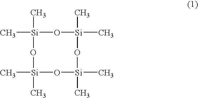
[0037]While, in the first embodiment described above, film-forming gas which contains OMCTS is used, different film-forming gas which contains, for example, tetramethyl cyclotetra siloxane (TMCTS) represented by the formula (2) given below may be used as the film-forming gas which has a ring structure of Si—O bonds. The TMCTS has a four-membered ring structure of Si—O bonds and is configured such that it has a CH3 group and H bonded to Si atoms which form the four-membered ring structure and further has Si—C bonds and Si—H bonds. Here, the Si—O bond has binding energy higher than those of the Si—C bond and the Si—H bond.

[0038]

[0039]Also in this instance, film-forming gas which contains, for example, TMCTS and O2 is used and the energy of pulse plasma discharge is controlled so that the four-membered ring structure of Si—O bonds is maintained while Si—C bonds are partly dissociated to form the interlayer insulating film 12. In this instance, since the Si—H bond has binding energy sub...

second embodiment

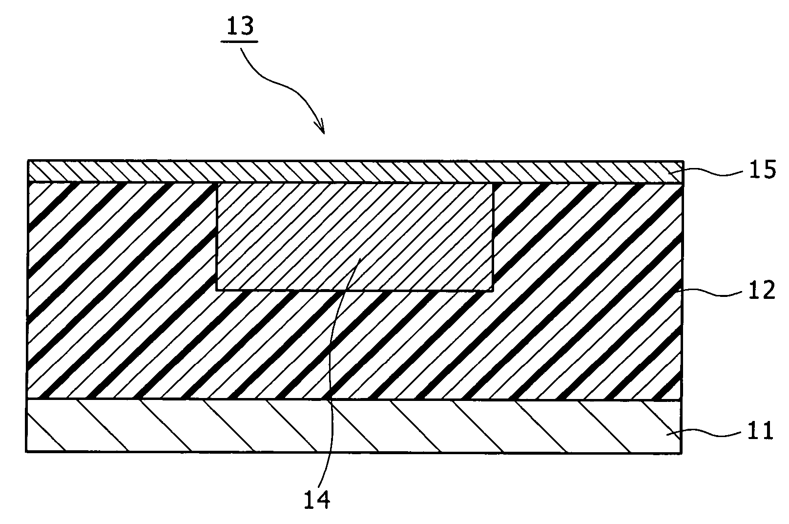
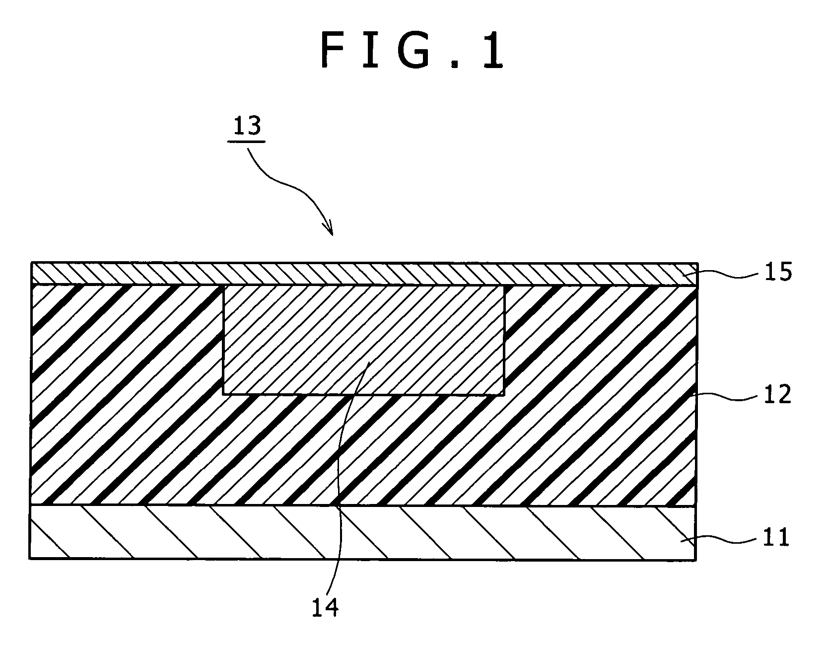
[0043]In the second embodiment of the present invention, film-forming gas different from that used in the first embodiment is used to form an interlayer insulating film 12 having a four-membered ring structure (cyclotetra siloxane) of Si—O bonds on a substrate 11. The film formation when the interlayer insulating film 12 is formed on the substrate 11 in the present embodiment can be performed using film-forming gas which contains silane (Si)-containing gas composed of, for example, trimethyl silane (3MS) represented by the formula (3) given below and O2 gas.

[0044]

[0045]Here, the formation of the interlayer insulating film 12 is performed by a plasma CVD method wherein the energy is controlled so that Si—C bonds in the 3MS are partly dissociated and Si and O2 react with each other in a vapor phase to form a four-member ring structure of Si—O bonds which are stable in structure and besides the formed four-member ring structure is maintained.

[0046]Consequently, since the interlayer ins...

modification 2

[0054]Further, such Si—O-containing gas formed from tetraethoxy silane (TEOS) as represented by the formula (4) may be used. Here, the TEOS includes four ethoxy (C2H5O) groups bonded to Si, and the Si—O bond has binding energy higher than that of the C—O bond.

[0055]

[0056]In this instance, TEOS gas and O2 are used as film-forming gas to form a four-membered ring structure of Si—O bonds in a vapor phase, and an interlayer insulating film 12 is formed by plasma discharge wherein the energy is controlled so that the ring structure of Si—O bonds is maintained while the C—O bonds are partly dissociated. Consequently, the interlayer insulating film 12 which has the four-membered ring structure of Si—O bonds is formed, and C-containing groups in the form of the ethoxy (C2H5O) group are introduced into the interlayer insulating film 12 at an introduction ratio with which a film strength can be maintained. Accordingly, effects similar to those of the second embodiment can be exhibited.

[0057]I...


PUM

PropertyMeasurementUnit
poweraaaaaaaaaa
dielectric constantaaaaaaaaaa

Abstract

A fabrication method of a semiconductor device is disclosed by which damage to another film or exfoliation of a film is prevented and an insulating film having a dielectric constant of 2.5 or less can be formed while a film strength is maintained without deteriorating a wiring line characteristic. According to an embodiment, an insulating film is formed on a substrate by a plasma process, which uses film-forming gas having a ring structure of Si—O bonds, such that it maintains the ring structure of the Si—O bonds. According to another embodiment, an insulating film is formed on a substrate by a plasma process, which uses film-forming gas which contains silane-containing gas and oxygen gas or film-forming gas which contains Si—O bond-containing gas, such that it has a ring structure of the Si—O bonds.

Description

RELATED APPLICATION DATA[0001]The present application claims priority to Japanese Application(s) No(s). P2004-200179 filed Jul. 7, 2004, which application(s) is / are incorporated herein by reference to the extent permitted by law.BACKGROUND OF THE INVENTION[0002]This invention relates to a fabrication method of a semiconductor device, and more particularly to a fabrication method of a semiconductor device having a multilayer wiring line structure wherein an insulating film having a dielectric constant lower than that of a silicon (Si) oxide film is used as an interlayer insulating film.[0003]In a multilayer wiring line structure of a CMOS semiconductor device, the problem of signal propagation delay has become conspicuous together with requirements for high speed processing and low power consumption of a device in recent years. In order to suppress increase of the signal propagation delay, it is necessary to achieve reduction in resistance of wiring lines and capacitance between wiri...

Claims


Application Information

Patent Timeline
Patent Type & Authority Patents(United States)
IPC IPC(8): H01L21/469
CPCC23C16/401C23C16/515H01L21/02126H01L21/02216H01L21/31633H01L21/0228H01L21/02362H01L21/31612H01L21/02274H01L21/31
Inventor TABUCHI, KIYOTAKA
Owner SONY CORP
Why Eureka
Try Eureka