Low power comsumption, low noise and high power gain distributed amplifiers for communication systems

a distributed amplifier and communication system technology, applied in the field of low power comsumption, low noise and high power gain distributed amplifiers for communication systems, can solve the problems of noise figure, design of 2 block circuits, and inapplicability to most such products, and achieve low power consumption, low noise, and high power gain.

Active Publication Date: 2009-08-25
UNITED MICROELECTRONICS CORP
View PDF9 Cites 32 Cited by
  • Summary
  • Abstract
  • Description
  • Claims
  • Application Information

AI Technical Summary

Benefits of technology

[0014]The present invention is to provide low power consumption, low noise and high power gain DA for communication systems, due to current re-use mechanism, and accordingly no output drain bias is needed.

Problems solved by technology

However, it challenges to design the 2 block circuits because of wide bandwidth, low noise, high gain, and low power consumption.
This has not been practical for most such products because of the power requirements associated with the transmitter's power output stage (sometimes referred to herein as a power amplifier) and low noise requirements associated with the receiver's low noise amplifier (LNA).
This caused the noise figure and poor linearity.

Method used


Image

  • Low power comsumption, low noise and high power gain distributed amplifiers for communication systems
  • Low power comsumption, low noise and high power gain distributed amplifiers for communication systems
  • Low power comsumption, low noise and high power gain distributed amplifiers for communication systems

Examples


Embodiment Construction

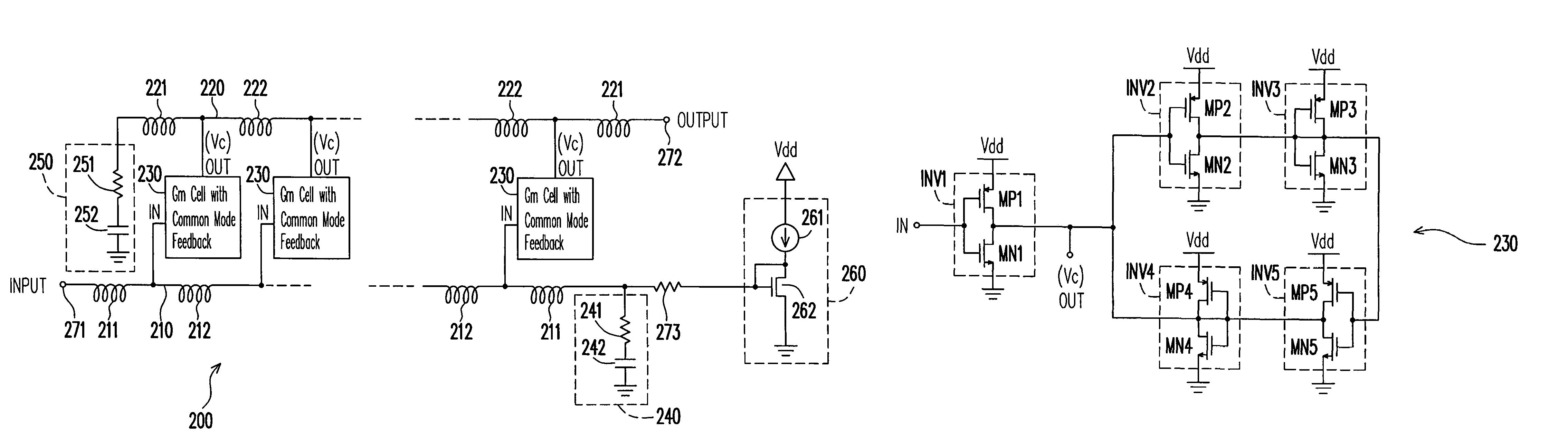
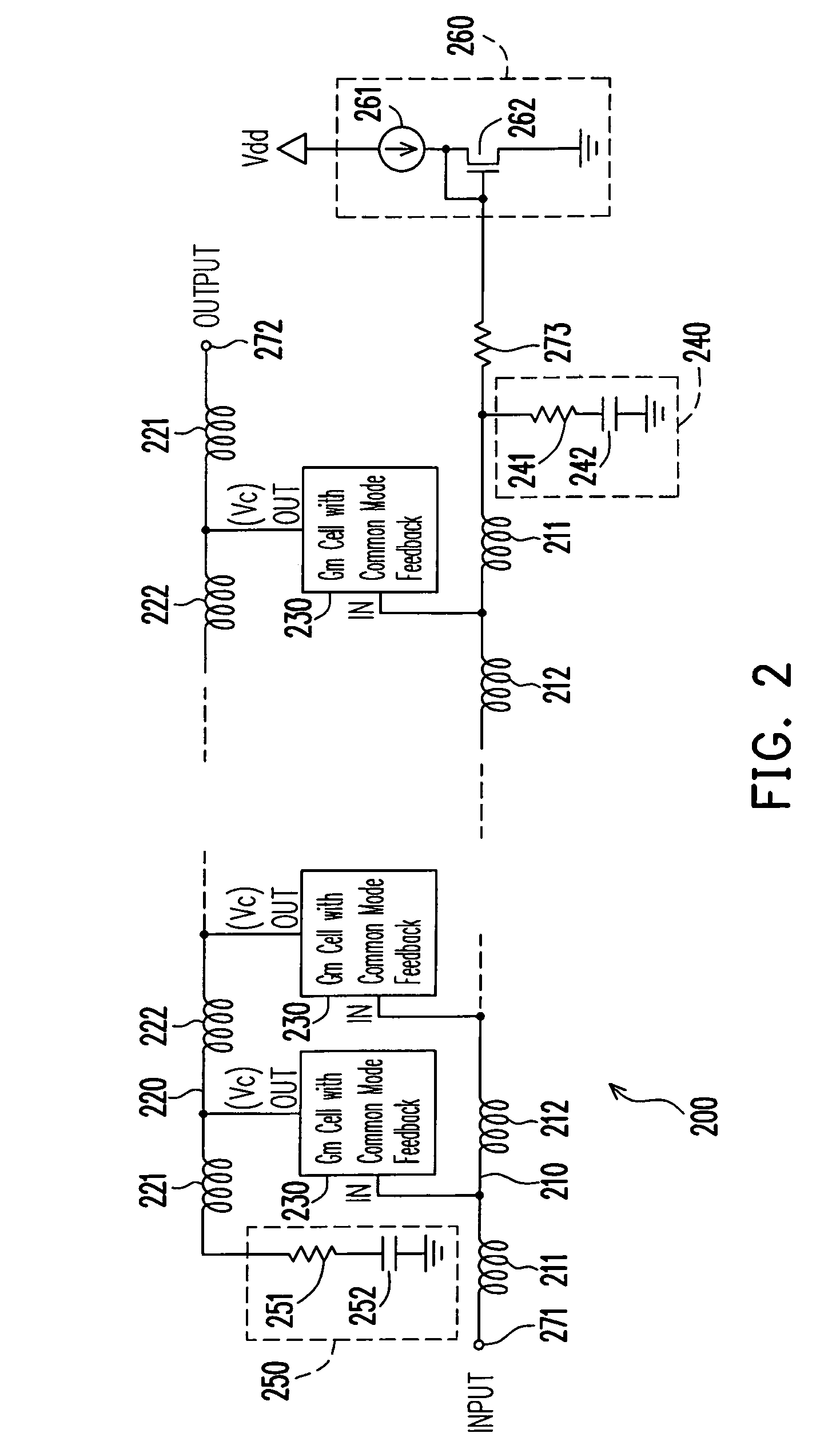
[0027]One of embodiments according to the invention shows the design and fabrication of a low power consumption, low noise and high power gain CMOS distributed amplifier (DA) for ultra-wideband (UWB) wireless applications. The proposed topology is implemented in CMOS MMRF technology and Process Design Kit (PDK). The measurement results show the amplifier achieves a flat forward gain (S21) of 8.3 dB and a noise figure as low as 3.3 dB over a wide bandwidth. S parameter S11 is lower than −15 dB for Mode 1 OFDM applications. The input 1 dB compression points (PldB) parameters are −5.8 dBm, −7.8 dBm, and −8 dBm when the input injected frequencies are at 2 GHz, 4 GHz, and 6 GHz, respectively. Biased by an internal negative resistance circuit, the power consumptions of the DA circuit are 29.8 mW under 1.2V power supply.

[0028]This embodiment according to the invention proposes a UWB DA based on Gm (transconductance) cells with common mode feedback to overcome the problems of linearity and ...


PUM


Abstract

Provided is a distributed amplifier in communication systems, including: an input transmission line; an output transmission line; an input impedance match and an output impedance match, for providing termination of the input transmission line and the output transmission line, respectively and for preventing signal reflection in the input transmission line and the output transmission line, respectively; multi-stage Gm cells with common mode feedback, the input transmission line being coupled to the output transmission line by the transconductance of the Gm cells; and an input gate bias circuit, for providing bias for the multi-stage Gm cells. In at least one of the Gm cells, one inverter performs V/I conversion while other inverters provide negative resistance to control common mode of output voltage and to enhance DC gain of the Gm cell. Due to common mode feedback, no output gate bias is needed.

Description

BACKGROUND OF THE INVENTION[0001]1. Field of Invention[0002]The present invention is directed generally to the field of electronic amplifiers, and particularly to distributed amplifiers (DA) for use in power output stages and / or receiving part of RF (Radio Frequency) communication products.[0003]2. Description of Related Art[0004]In communication systems such as RF transceivers, it is desirable to integrate as much circuitry as possible on a single semiconductor chip. The main function blocks in the RF transceivers are Low Noise Amplifier (LNA) in the receiver part and Power Amplifier (PA) in the transmitter part. However, it challenges to design the 2 block circuits because of wide bandwidth, low noise, high gain, and low power consumption.[0005]This has not been practical for most such products because of the power requirements associated with the transmitter's power output stage (sometimes referred to herein as a power amplifier) and low noise requirements associated with the rec...

Claims


Application Information

Patent Timeline
Patent Type & Authority Patents(United States)
IPC IPC(8): H03F3/60
CPCH03F3/605H03F2203/45212
Inventor CHENG, YUYEN, ALBERT KUO-HUEICHANG, JEN-CHUNG
Owner UNITED MICROELECTRONICS CORP
Why Eureka
Try Eureka