
Nonvolatile memory

a non-volatile memory, non-volatile technology, applied in the direction of digital storage, instruments, semiconductor devices, etc., can solve the problems of lower reliability, lower integration degree and cost, and power consumption that is larger than that of the full-function eeprom, so as to achieve low cost and small size

Inactive Publication Date: 2009-09-29
SEMICON ENERGY LAB CO LTD
View PDF20 Cites 5 Cited by
  • Summary
  • Abstract
  • Description
  • Claims
  • Application Information

AI Technical Summary

Benefits of technology

[0013]It is an object of the present invention to provide a nonvolatile memory which is capable of realizing higher integration.
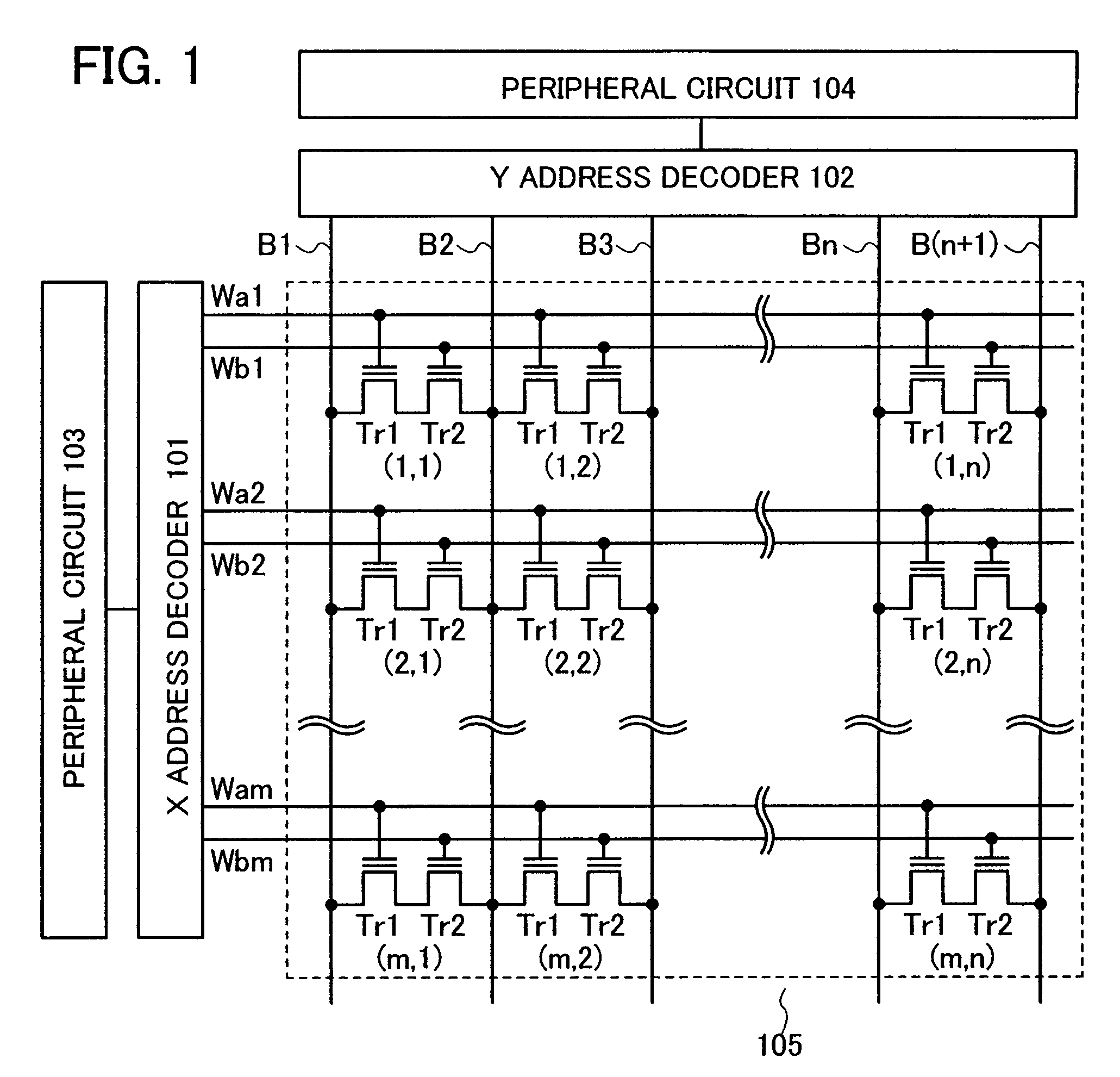
[0018]In the nonvolatile memory of the present invention, a memory cell includes two memory transistors, a conventional source line is excluded, and each memory transistor is connected to a bit line which is adjacent thereto instead of the conventional source line. Accordingly, a full-function EEPROM of which integration density is high, size is small, and cost is low can be provided.

Problems solved by technology

The full-function EEPROM has higher functions while it is inferior in integration degree and cost as compared to the flash memory.
This makes the power consumption larger than that of the full-function EEPROM and lowers the reliability because data is rewritten even in a memory cell where data rewriting is not needed.
Of course, the flash memory cannot be used for an application that needs an erasing operation for each bit.
However, the full-function EEPROM has a problem in that a memory cell area is large and the integration density is low because each memory cell in which 1-bit data is stored includes two transistors, that are the memory transistor and the selection transistor.
This obstructs reduction in size and cost of the full-function EEPROM.

Method used


Image

  • Nonvolatile memory
  • Nonvolatile memory
  • Nonvolatile memory

Examples


embodiment mode 1

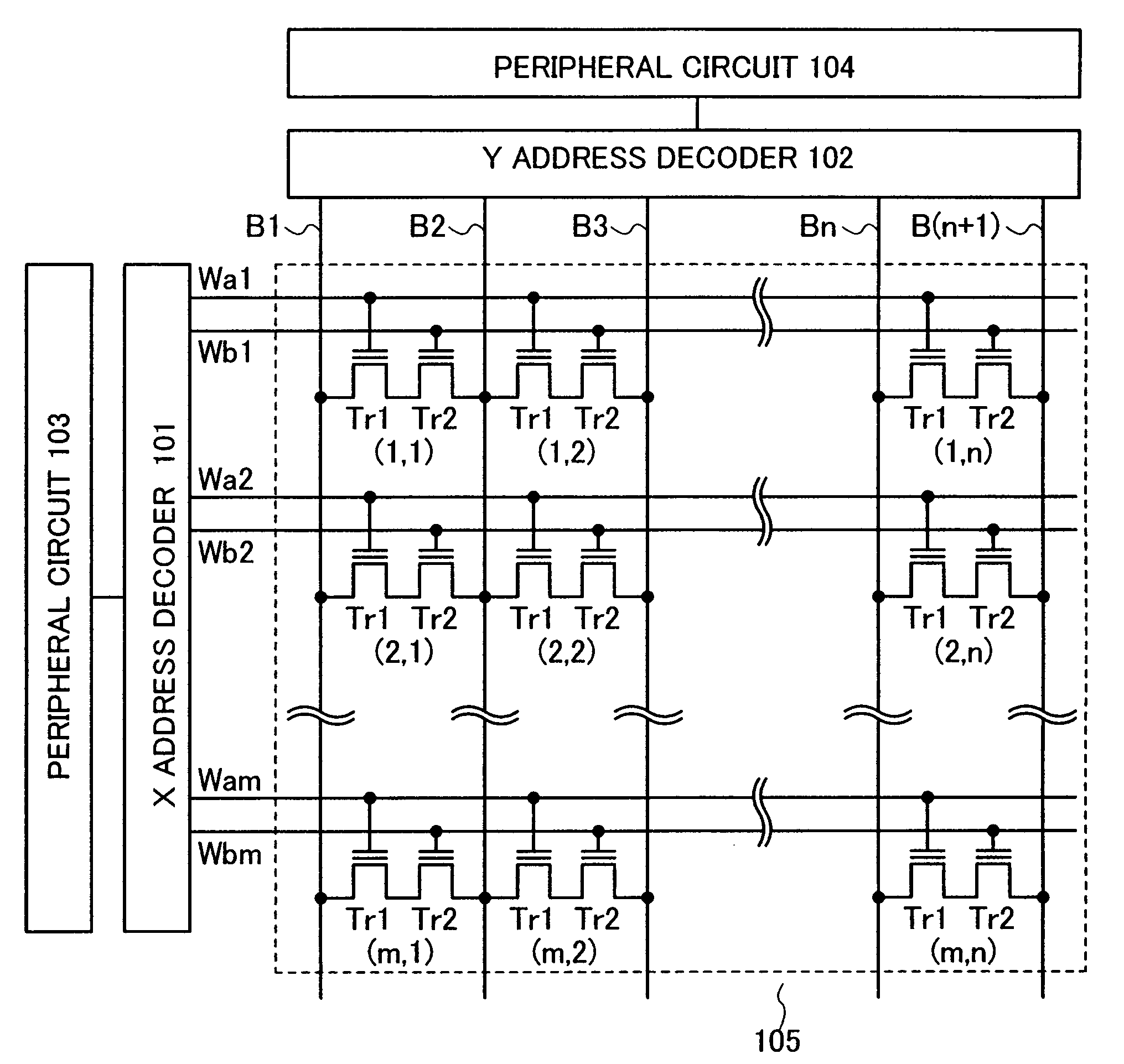
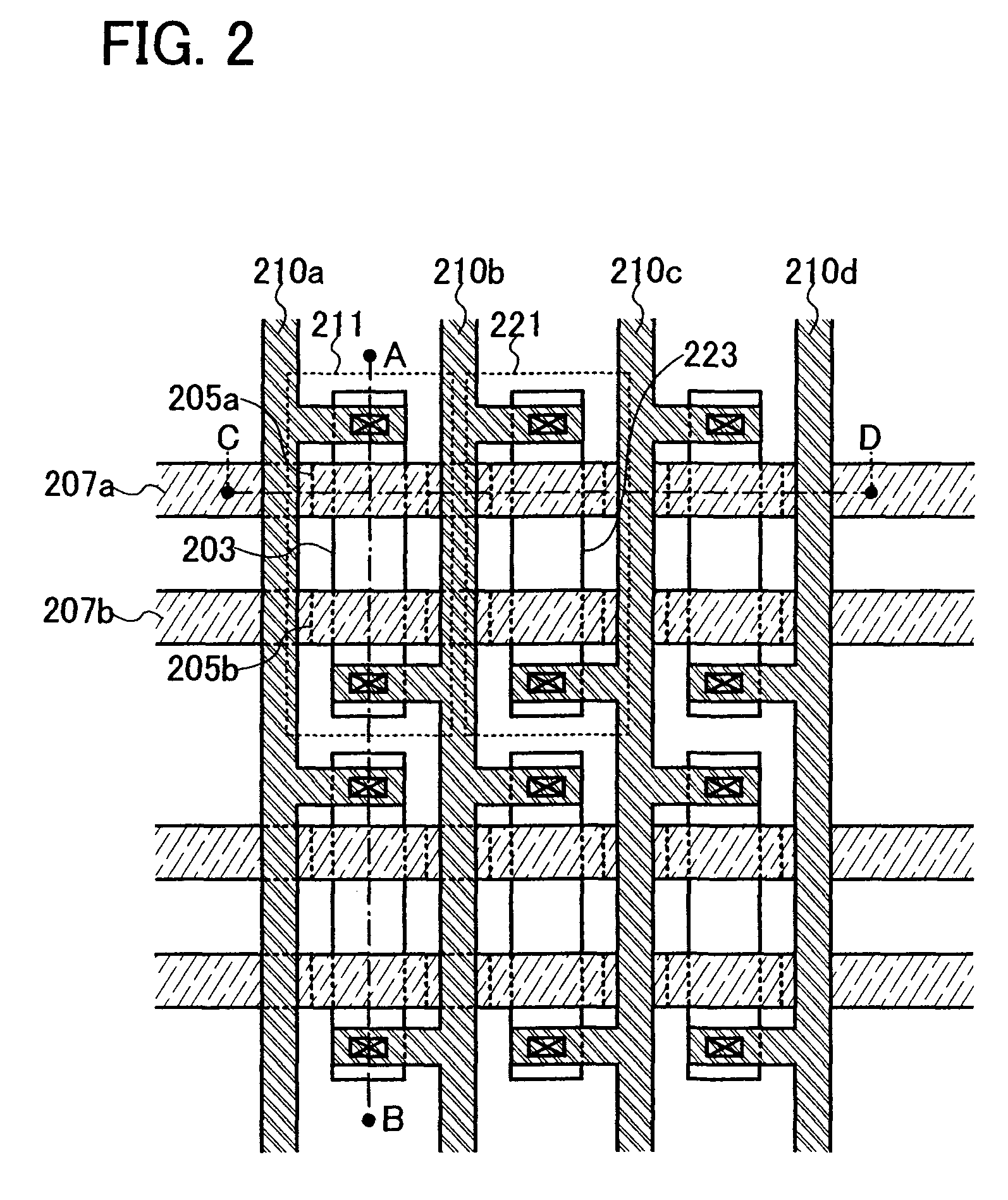
[0035]This embodiment mode describes a circuit diagram, a driving method, and a cross-sectional structure of a memory cell, of a nonvolatile memory of the present invention.

[0036]FIG. 1 shows circuits of a nonvolatile memory described in this embodiment mode. Shown as an example here is a circuit diagram of a (m×n)-bit nonvolatile memory (m and n are integers which are greater than or equal to 1).

[0037]The nonvolatile memory described in this embodiment mode includes a memory cell array 105 in which (m×n) memory cells (1, 1) to (m, n) are arranged in matrix so as to be m memory cells in row and n memory cells in column, an X address decoder 101 and a Y address decoder 102 which are driver circuits of the memory cell array 105, and other peripheral circuits 103 and 104.

[0038]Each memory cell (typically, a memory cell (i, j) is considered) (i is an integer which is greater than or equal to 1 and less than or equal to m, and j is an integer which is greater than or equal to 1 and less ...

embodiment mode 2

[0084]This embodiment mode describes a 2048-bit nonvolatile memory which includes p-channel transistors is described as an example of the nonvolatile memory of the present invention with reference to the drawing.

[0085]FIG. 11 is a circuit diagram of the nonvolatile memory of this embodiment mode. The nonvolatile memory shown in FIG. 11 includes a memory cell array 605 in which 1,024 memory cells (1, 1) to (32, 32) are arranged in matrix so as to be 32 memory cells in column and 32 memory cells in row, an X address decoder 601, a Y address decoder 602, and other peripheral circuits 603 and 604. Each memory cell includes two p-channel transistors Tr1 and Tr2. In the case where 1-bit data is stored in each memory transistor, the nonvolatile memory of this embodiment mode has a storage capacity of 2048 bits. The above-described other peripheral circuits include an address buffer circuit, a control logic circuit, a sense amplifier, a voltage step-up circuit, and the like, which are provi...

embodiment mode 3

[0096]This embodiment mode describes one example of a manufacturing method of the nonvolatile memory of the present invention with reference to the drawings. Note that in the description below, as elements included in the nonvolatile memory, two memory transistors (n-channel memory TFTs) provided in a memory cell and two thin film transistors (a p-channel TFT and an n-channel TFT) included in a CMOS circuit which is a driver circuit of the memory cells or another peripheral circuit are described.

[0097]First, island-shaped semiconductor films 808, 810, and 812 are formed over a substrate 802 with an insulating film 804 interposed therebetween (FIG. 7A). The island-shaped semiconductor films 808, 810, and 812 can be provided as follows: an amorphous semiconductor film is formed of a material containing silicon (Si) as its main component (e.g., SixGe1-x) by a sputtering method, an LPCVD method, a plasma CVD method, or the like over the insulating film 804 formed in advance over the sub...


PUM


Abstract

A highly-integrated nonvolatile memory. A memory cell array where plural memory cells are arranged in matrix in row and column directions, plural first and second word lines, and plural bit lines are included. Each of the plural memory cells includes a first memory transistor and a second memory transistor which are connected in series. A gate electrode of the first memory transistor is connected to the first word line, a gate electrode of the second memory transistor is connected to the second word line, one of source and drain regions of the first memory transistor is connected to the first bit line, and one of source and drain regions of the second memory transistor is connected to the second bit line. Each of the first bit line and the second bit line is provided in common for memory cells in columns which are adjacent to each other.

Description

BACKGROUND OF THE INVENTION[0001]1. Field of the Invention[0002]The present invention relates to a semiconductor nonvolatile memory. In particular, the present invention relates to an electrically writable and erasable semiconductor nonvolatile memory (EEPROM: Electrically Erasable and Programmable Read Only Memory).[0003]2. Description of the Related Art[0004]In recent years, there has rapidly spread a small semiconductor device with multiple functions and high performance, which is represented by a mobile appliance such as a mobile computer or a mobile phone. Accordingly, a semiconductor nonvolatile memory has been noted as a memory included in a semiconductor device. The semiconductor nonvolatile memory is characteristically superior in integration density, shock resistance, power consumption, writing / reading speed, or the like while it is inferior in storage capacity, to a magnetic disk. In recent years, there has been developed a semiconductor nonvolatile memory which has suffi...

Claims


Application Information

Patent Timeline
Patent Type & Authority Patents(United States)
IPC IPC(8): G11C16/04
CPCG11C8/10G11C8/12G11C8/14G11C16/0458H01L27/115H01L27/11526H01L27/11546H01L27/12G11C16/0491H01L27/124H10B41/40H10B41/49H10B69/00G11C16/14G11C16/16G11C16/24G11C16/08
Inventor KATO, KIYOSHIYAMAZAKI, SHUNPEI
Owner SEMICON ENERGY LAB CO LTD
Learn More