Current-controlled CMOS (C3MOS) fully differential integrated wideband amplifier/equalizer with adjustable gain and frequency response without additional power or loading

a wideband amplifier and wideband equalizer technology, applied in the field of communication devices, can solve the problems of adding a significant amount of parasitic loading to the high speed data path, consuming a significant amount of power, and being power hungry

Inactive Publication Date: 2009-10-06
AVAGO TECH INT SALES PTE LTD +1
View PDF184 Cites 33 Cited by
  • Summary
  • Abstract
  • Description
  • Claims
  • Application Information

AI Technical Summary

Problems solved by technology

For transmission rates of 10 Gbps (Giga-bits per second) or higher, the data amplifier or equalizer generally consume a significant amount of power.
The summer is especially power hungry because it has two pairs of full-rate data input.
This adds a significant amount of parasitic loading to the high speed data path.
This has the undesirable effect and deleterious effect of reducing the bandwidth of the data path.
Moreover, if the combined input is connected to the input pads of the receiver directly, it will cause a severe degradation of the impedance matching (i.e., will cause a severe impedance mis-match) between the input of the receiver and the traces on the PCB (Printed Circuit Board) due to the excessive capacitance loading.
This results in even more undesirable and deleterious effects due to the large amount of reflections, and this significantly degrades the integrity of the input data.
Another potential issue and problem of this prior art two path embodiment 100 is when the signals that pass through the two different paths are ultimately combined together at the summer, it may generate addition jitter if the delay between the two path differs significantly.
As can be seen, while this prior art two path embodiment 100 does provide at least one solution to having an adjustable gain and equalizer stage, it has significant limitations.
More specifically, among other problems, this prior art two path embodiment 100 significantly power consumptive, it may introduce undesirable impedance matches, and it may require great care be taken to ensure the two paths have substantially similar delays.

Method used


Image

  • Current-controlled CMOS (C3MOS) fully differential integrated wideband amplifier/equalizer with adjustable gain and frequency response without additional power or loading
  • Current-controlled CMOS (C3MOS) fully differential integrated wideband amplifier/equalizer with adjustable gain and frequency response without additional power or loading
  • Current-controlled CMOS (C3MOS) fully differential integrated wideband amplifier/equalizer with adjustable gain and frequency response without additional power or loading

Examples


embodiment 300

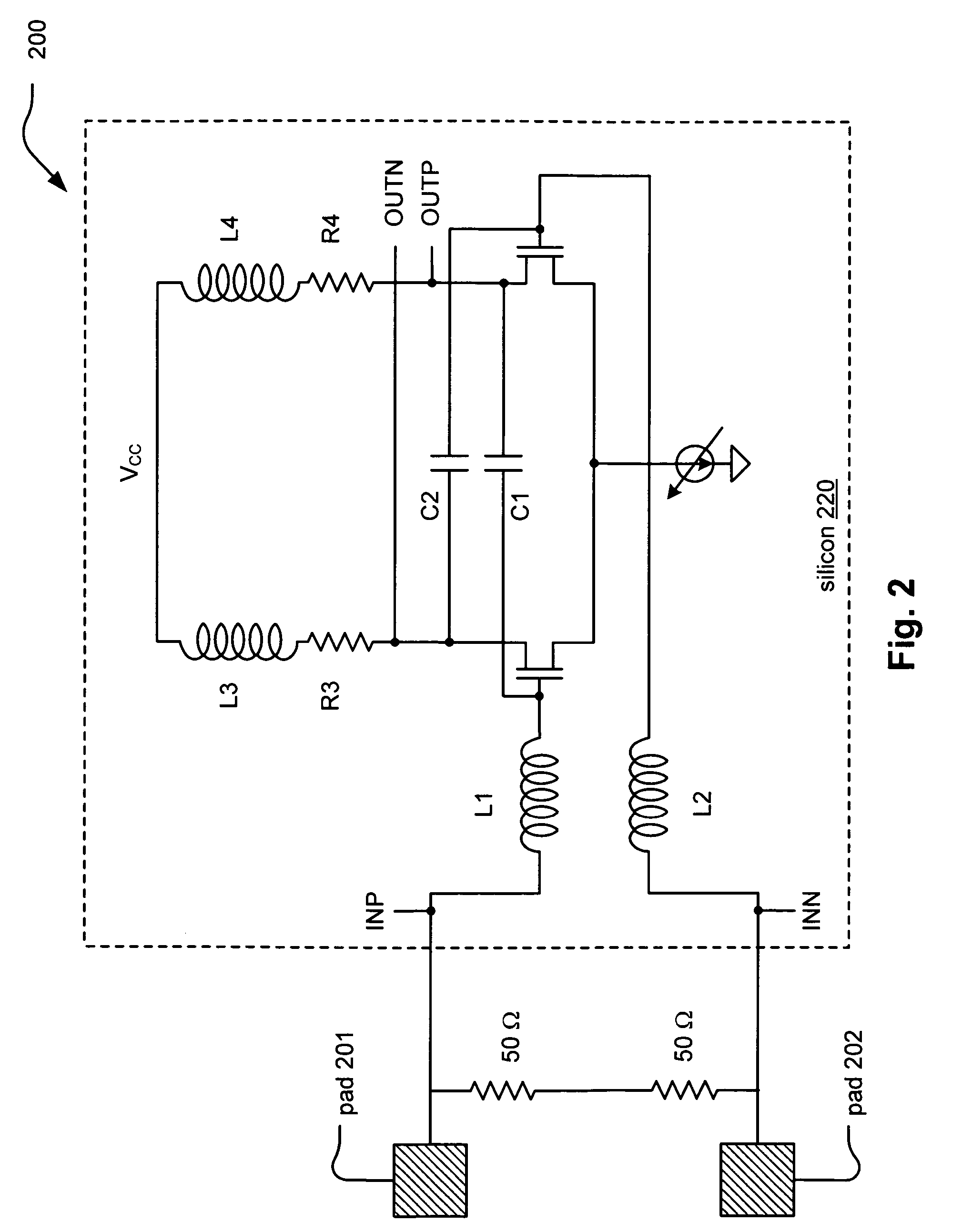
[0037]FIG. 3 illustrates an embodiment 300 of a C3MOS wideband data amplifier / equalizer circuit 310 with adjustable gain and frequency response without additional power or loading.

[0038]A novel approach is presented by which an adjustable amplifier / equalizer stage may be implemented without suffering from many of the undesirable and deleterious effects described above with respect to a two path embodiment 100 of an adjustable amplifier / equalizer. One of the many advantages of this new design is that all the bandwidth extension techniques existent in the context of C3MOS wideband data amplifiers can be readily applied to a C3MOS wideband data integrated amplifier / equalizer stage.

[0039]In FIG. 3, series input impedances 321 and 322, output impedances 331 and 332 are all added so that the stage can achieve high bandwidth with a minimum increase in power consumption. If desired, as is shown below within other embodiment, and negative Miller capacitors may also be employed. The input imp...

embodiment 1001

[0062]It is also noted that for each of the embodiments 901 of the FIG. 9A and 902 of the FIG. 9B, the resistors and MOSFETs can be switched. Specifically, in the FIG. 9A, the branches controlled by the signals CNTRL2, CNTRL3, CNTRL4, . . . CNTRLn can be modified such that each of the resistors therein can be replaced by a MOSFET, and the MOSFETs therein can be replaced by resistors. This configuration is depicted in embodiment 1001 of FIG. 10A.

[0063]Analogously, in the FIG. 9B, the branches controlled by the signals CNTRL2, CNTRL3, CNTRL4, . . . CNTRLn can be modified such that each of the capacitors therein can be replaced by a MOSFET, and the MOSFETs therein can be replaced by capacitors. This configuration is depicted in embodiment 1002 of FIG. 10B.

[0064]Referring to FIG. 11A, this diagram is largely a combination 1101 of the FIG. 9A and the FIG. 9B (without including the variable capacitor or the variable resistor). The FIG. 11A includes an array of corporately (and individuall...

embodiment 1200

[0067]FIG. 12 illustrates an embodiment 1200 of implementation of one or more C3MOS wideband data amplifier / equalizer circuits within a communication transceiver that communicatively couples to a communication network.

[0068]This diagram shows a communication transceiver 1210 that may be implemented in any of a wide variety of communication systems. For example, the communication transceiver 1210 may communicatively couple to and communicate with an Ethernet network 1299. Such an Ethernet network 1299 may be implemented as a fiber-optic network; generally speaking, the Ethernet network 1299 may also be implemented as a wired network or a combination network that includes both wired and wireless components. As desired, the communication transceiver 1210 may be implemented to perform bi-directional communication with a wide variety of communication system types. In addition, the communication transceiver 1210 may be implemented as a single integrated circuit in some embodiments. Altern...


PUM


Abstract

Current-controlled CMOS (C3MOS) fully differential integrated wideband amplifier / equalizer with adjustable gain and frequency response without additional power or loading. A novel approach is presented by which adjustable amplification and equalizer may be achieved using a C3MOS wideband data stage. This may be referred to as a C3MOS wideband data amplifier / equalizer circuit. This employs a wideband differential transistor pair that is fed using two separate transistor current sources. A switchable RC network is communicatively coupled between the sources of the individual transistors of the wideband differential transistor pair. There are a variety of means by which the switchable RC network may be implemented, including using a plurality of components (e.g., capacitors and resistors connected in parallel). In such an embodiment, each component may have an individual switch to govern its connectivity in the switchable RC network thereby allowing a broad range of amplification and equalization to be performed.

Description

CROSS REFERENCE TO RELATED PATENTS / PATENT APPLICATIONSProvisional Priority Claims[0001]The present U.S. Patent Application claims priority pursuant to 35 U.S.C. § 119(e) to the following U.S. Provisional Patent Application which is hereby incorporated herein by reference in its entirety and made part of the present U.S. Utility Patent Application for all purposes:[0002]1. U.S. Provisional Application Ser. No. 60 / 704,134, entitled “Current-controlled CMOS (C3MOS) fully differential integrated wideband amplifier / equalizer with adjustable gain and frequency response without additional power or loading,” filed Friday, Jul. 29, 2005.Incorporation by Reference[0003]The following U.S. Utility Patent Applications are hereby incorporated herein by reference in their entirety and made part of the present U.S. Utility Patent Application for all purposes:[0004]1. U.S. patent application Ser. No. 09 / 484,856, entitled “Current-controlled CMOS logic family,” filed Jan. 18, 2000, now U.S. Pat. No. ...

Claims


Application Information

Patent Timeline
Patent Type & Authority Patents(United States)
IPC IPC(8): H03F3/191H03F3/45
CPCH03F3/45183H03F3/45197H03G1/0088H03G1/0029H03F2200/405H03F2203/45134H03F2203/45332H03F2203/45504H03F2203/45554H03F2203/45638H03F2203/45702H03F2203/45466
Inventor CAO, JUN
Owner AVAGO TECH INT SALES PTE LTD
Why Eureka
Try Eureka