Micromachining with short-pulsed, solid-state UV laser

a laser and micromachining technology, applied in the field of laser micromachining, can solve the problems of micromachining parameters of q-switched lasers, including their wavelengths (ranging from near infrared to deep ultraviolet), pulse energy, pulse repetition rate, etc., and achieve the effect of increasing the throughput of laser micromachining

Active Publication Date: 2009-10-20
ELECTRO SCI IND INC
View PDF43 Cites 39 Cited by
  • Summary
  • Abstract
  • Description
  • Claims
  • Application Information

AI Technical Summary

Benefits of technology

[0014]In some exemplary embodiments, the number of pulses employed to clean an underlying pad is significantly reduced, and in most preferred cases only one pulse is employed for cleaning.

Problems solved by technology

However, micromachining parameters for Q-switched lasers, including their wavelengths (ranging from near infrared to deep ultraviolet), pulsewidths, pulse energies, and pulse repetition rates, have still not been perfected for certain classes of layered organic, inorganic, and metallic microelectronic material constructions with respect to throughput and machining quality, such as cleanness, sidewall taper, roundness, and repeatability.

Method used


Image

  • Micromachining with short-pulsed, solid-state UV laser
  • Micromachining with short-pulsed, solid-state UV laser
  • Micromachining with short-pulsed, solid-state UV laser

Examples


Embodiment Construction

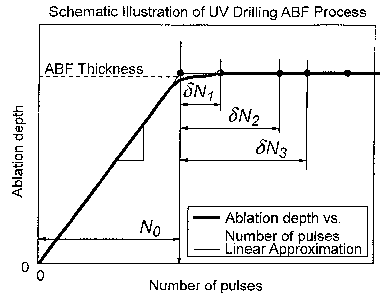
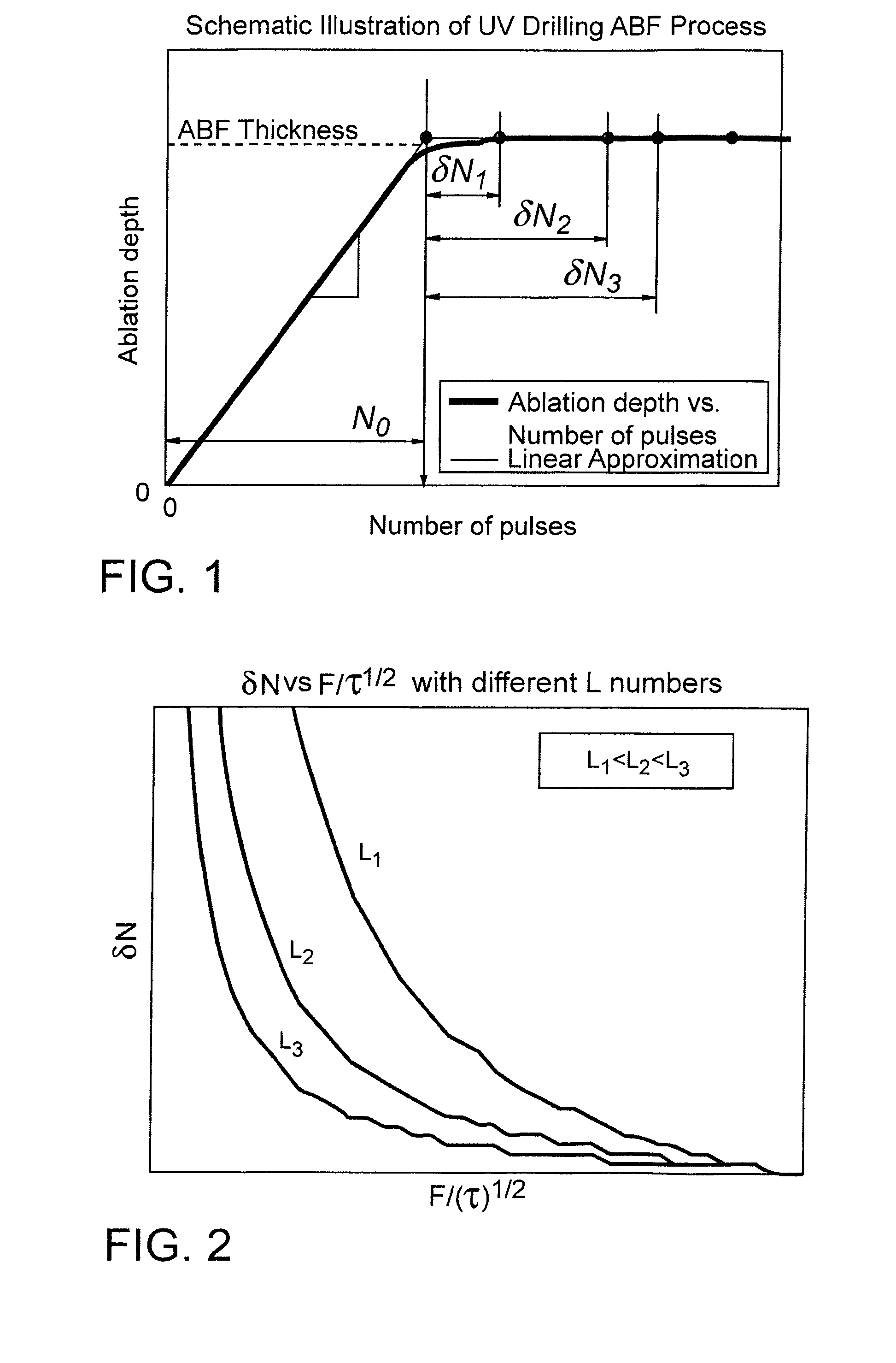
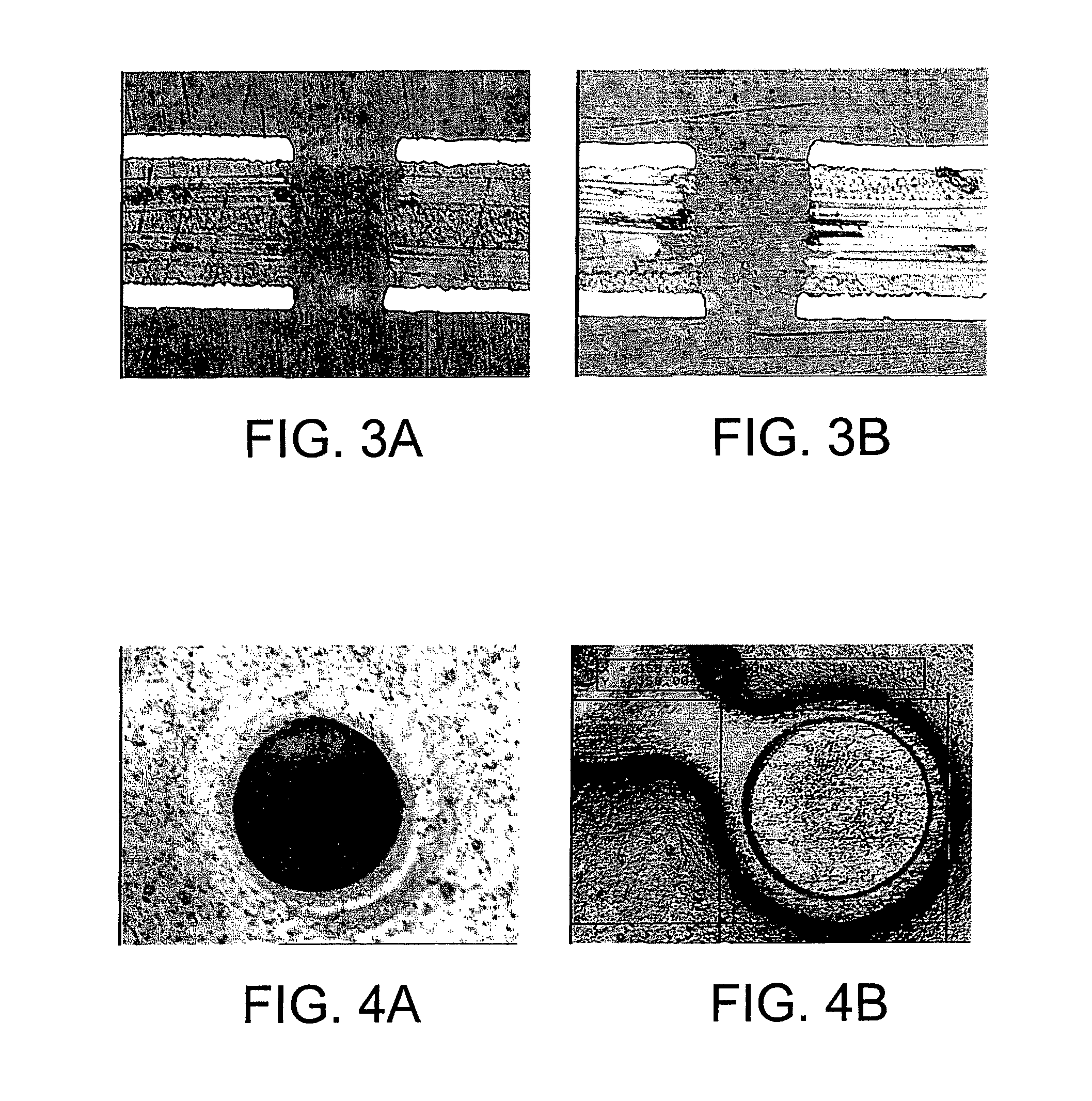
[0027]Preferred embodiments entail the use of a solid-state UV laser to perform via drilling and ablation of electronic circuit materials such as homogenous films, particulate-filled resins, polyimides, and fiber-reinforced polymers, with or without metal cladding. An Ajinomoto build-up film (ABF®) circuit-board dielectric material manufactured by Ajinomoto Fine-Techno Co., Inc., Kawasaki, Japan, is typical of a target material upon which via drilling operations may be performed. Some exemplary workpieces include ABF® SH-9K, ABF® GX-3, ABF® GX-13, or similar products manufactured by other companies, but other via drilling target materials (including, but not limited to, multilayered, laminated substrates such as those used in high-density printed wiring boards and integrated circuit chip packages are also suitable for processing in accordance with the exemplary embodiments disclosed herein.

[0028]Workpieces intended for via drilling typically contain conductive cladding layers that m...


PUM

PropertyMeasurementUnit
wavelengthaaaaaaaaaa

Abstract

In some embodiments, laser output including at least one laser pulse having a wavelength shorter than 400 microns and having a pulsewidth shorter than 1,000 picoseconds permits the number of pulses used to clean a bottom surface of a via or the surface of a solder pad to increase process throughput. An oscillator module in cooperation with an amplification module may be used to generate the laser output.

Description

TECHNICAL FIELD[0001]The invention relates to laser micromachining and, in particular, to laser micromachining applications with a short-pulsed laser.BACKGROUND OF THE INVENTION[0002]Q-switched solid-state lasers are well known and have been demonstrated successfully for many laser micromachining applications. However, micromachining parameters for Q-switched lasers, including their wavelengths (ranging from near infrared to deep ultraviolet), pulsewidths, pulse energies, and pulse repetition rates, have still not been perfected for certain classes of layered organic, inorganic, and metallic microelectronic material constructions with respect to throughput and machining quality, such as cleanness, sidewall taper, roundness, and repeatability.[0003]One such class of materials, commonly used in the printed wiring board (PWB) industry, includes glass cloth impregnated with one or more organic polymer resins that is sandwiched between conductive metal layers, typically copper. This mate...

Claims


Application Information

Patent Timeline
Patent Type & Authority Patents(United States)
IPC IPC(8): B23K26/38
CPCB23K26/0635B23K26/4095B23K26/386H05K3/0035B23K26/4005B23K26/401B23K26/4015B23K26/402B23K26/403B23K26/4065B23K26/408B23K26/409B23K26/381B23K2201/40H05K3/0038H05K3/28B23K26/40B23K26/382B23K26/0624B23K26/389B23K2101/35B23K2101/40B23K2103/08B23K2103/10B23K2103/12B23K2103/14B23K2103/172B23K2103/26B23K2103/42B23K2103/50B23K2103/52B23K26/00B23K26/36H01S3/10B23K26/38
Inventor LEI, WEISHENGSIMENSON, GLENNMATSUMOTO, HISASHIDAVIGNON, JOHN
Owner ELECTRO SCI IND INC
Why Eureka
Try Eureka