Siloxane-polymer dielectric compositions and related organic field-effect transistors

a technology of organic field-effect transistors and dielectric compositions, which is applied in the direction of organic chemistry, coatings, thermoelectric devices, etc., can solve the problems of high operating voltage, damage to organic components, and high operating voltage of otfts, and achieve low current leakage and good saturation characteristics

Inactive Publication Date: 2009-10-20
NORTHWESTERN UNIV
View PDF14 Cites 48 Cited by
  • Summary
  • Abstract
  • Description
  • Claims
  • Application Information

AI Technical Summary

Problems solved by technology

However, the resulting OTFTs are limited by high operating voltages, typically >>10 V, due to the intrinsic low carrier mobilities of the semiconductors and the low capacitances of the dielectrics (typically thick SiO2 and polymer films).
One approach to reducing OTFT operating voltages is to employ relatively thick, conventional high-dielectric constant oxide films, however, the vapour-phase deposition processes typically employed (e.g., sputtering) risk damaging organic components and yielding poor mechanical properties on flexible substrates.
Furthermore, ultra-thin inorganic insulators are typically electrically “leaky”, rendering them incompatible with low-mobility semiconductors.
However, reported capacitances are again modest (˜3 nF cm−2) for low-voltage OTFT applications.
This represents a significant advance, however the polymerization / annealing temperatures are quite high (230-290° C.) and the reported device I-V saturation characteristics not ideal.

Method used


Image

  • Siloxane-polymer dielectric compositions and related organic field-effect transistors
  • Siloxane-polymer dielectric compositions and related organic field-effect transistors
  • Siloxane-polymer dielectric compositions and related organic field-effect transistors

Examples


example 1

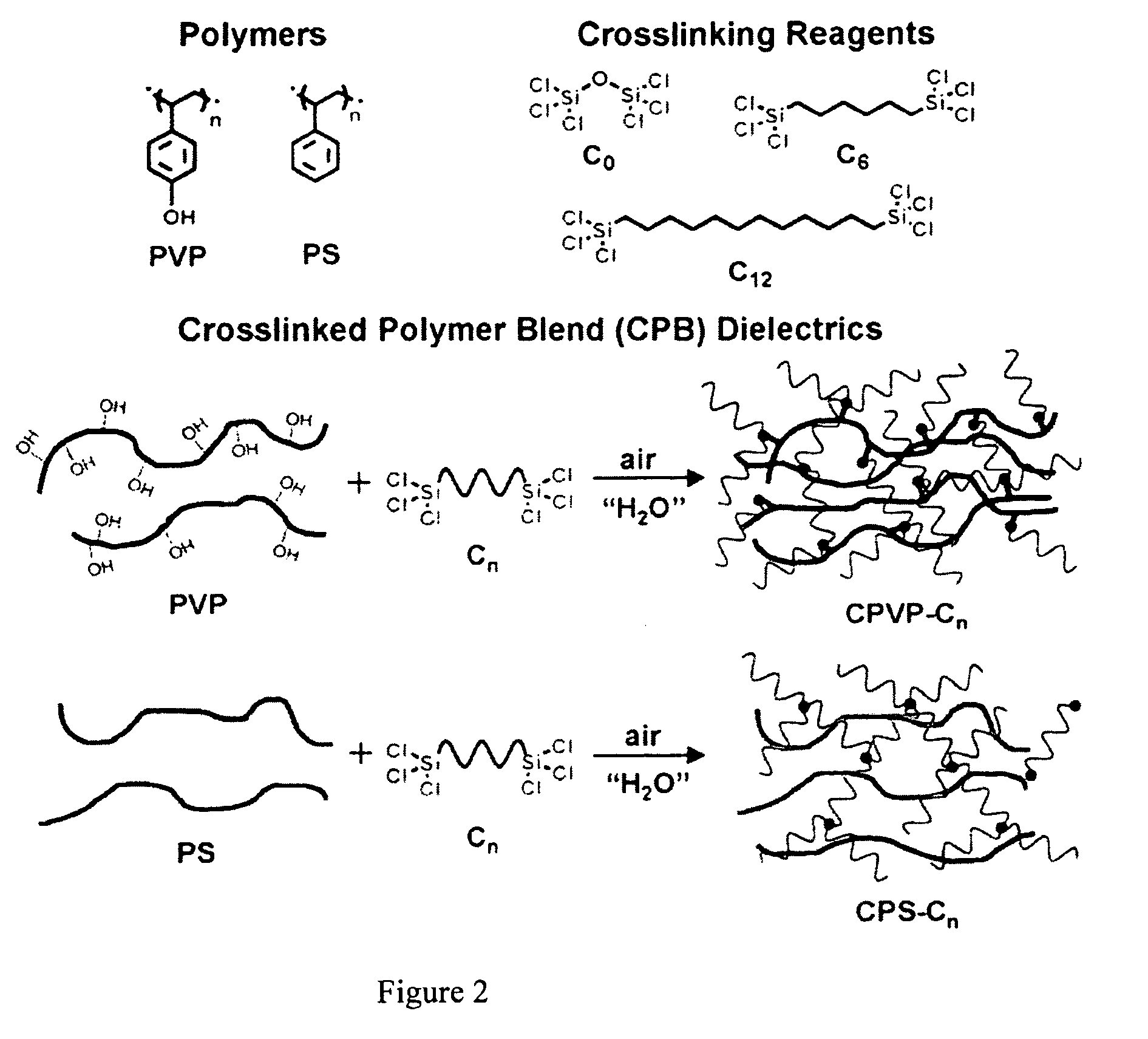
[0045]Dielectric coating. Using the aforementioned CPB designation, for crosslinked PVP, CPVP-Cn (n=0, hexachlorosiloxane; 6, 1,6-bis(trichlorosilyl)hexane; 12, 1,12-bis(trichlorosilyl)dodecane)), PVP (4 mg / mL in anhydrous THF) was mixed with the trichiorosilyl reagent (4 mg / rnL in anhydrous THF) in a 1:1 volume ratio and then spin-coated onto freshly oxygen plasma-treated Si (ITO-glass, ITO-Mylar, or Al) substrates at 5000 rpm (acceleration 60), and then cured in vacuum oven at 100-110.degree. C. for 5-10 min. For crosslinked polystyrene (PS), CPS-Cn, polystyrene (Mw=1M; 7 mg / mL in anhydrous toluene) was mixed with the trichlorosilyl reagent in anhydrous toluene in a 1:1 volume ratio, was then diluted with 2 parts of toluene, and then spin-coated onto substrates at 4000 rpm (acceleration 60), and cured in vacuum oven at 100-110° C. overnight. PVP-only and PS-only films for capacitance measurements were spin-coated from 20 mg / mL THE and toluene solutions, respectively, at 2500 rpm a...

example 2

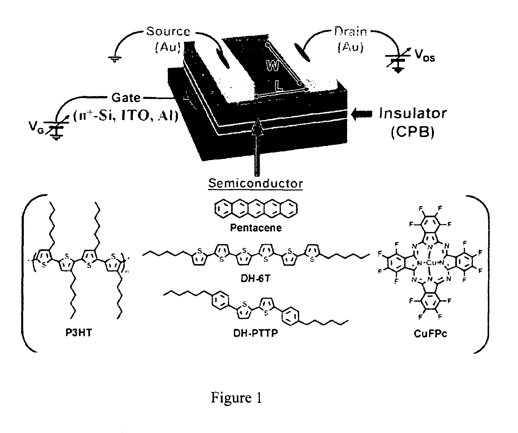
[0046]Device fabrication. For OTFTs, organic semiconducting materials were vacuum deposited at ˜2×10⁻⁶ Torr (500 Å, 0.2 Å / s) while maintaining the substrate temperature at 60° C. Films of P3HT, for instance, were spin-coated from a dry toluene solution (1 weight %, 2000 rpm) at RT. Gold electrodes for OTFT / MIS / MIM devices were vacuum-deposited through shadow masks at 3-4×10⁻⁶ Torr (1000 Å, 0.5 Å / s). Regardless of device configuration, the compositions of this invention can be used with a range of other semiconductor materials known in the art, including but not limited to, n-type and p-type polythiophene compounds of the sort described in U.S. Pat. No. 6,585,914, the entirety of which is incorporated herein by reference.

example 3

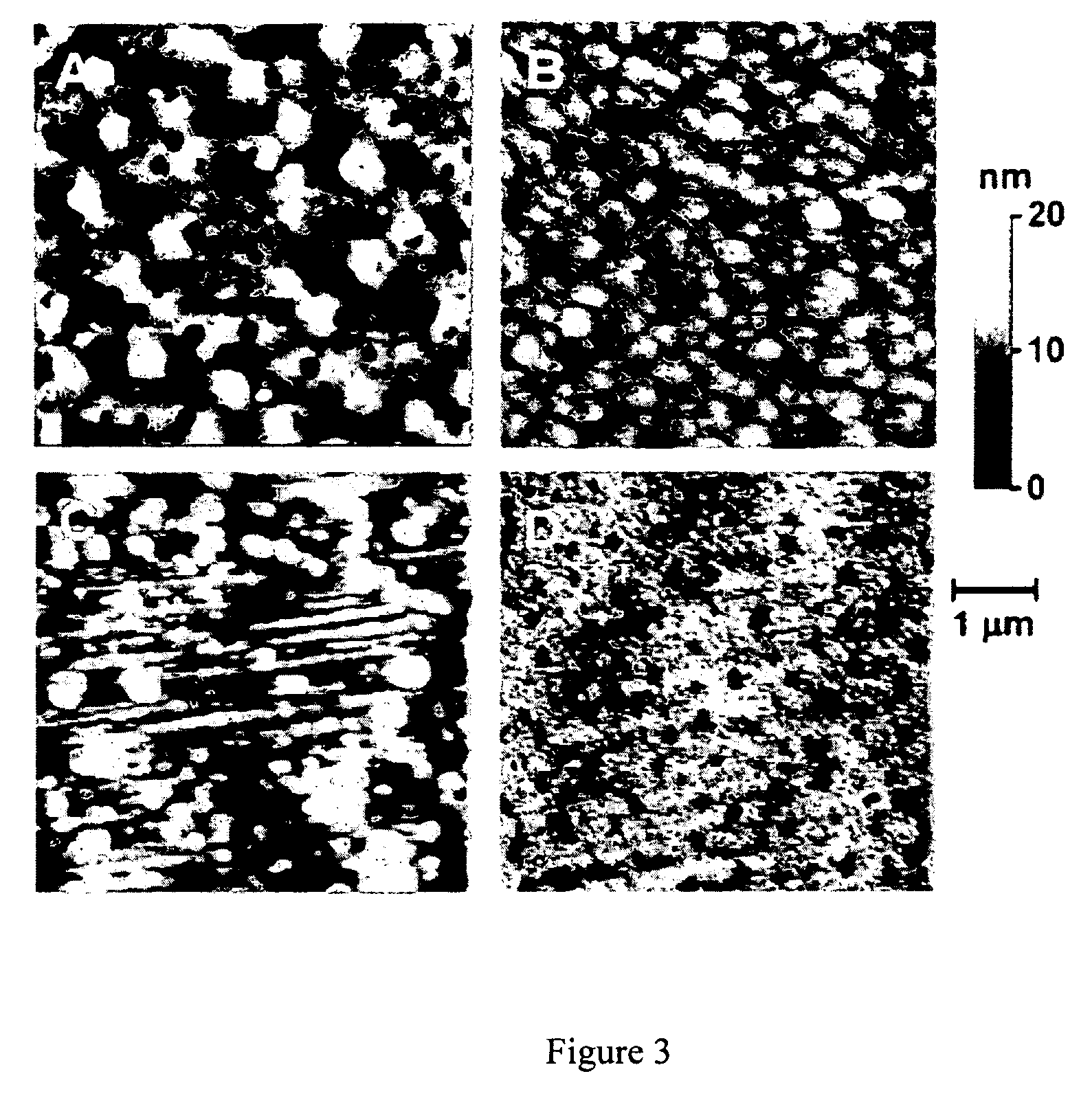
[0047]To assess the influence of differing CPB structures (FIG. 2) and to highlight the effects of polymer microstructure and crosslinker on dielectric film properties, two polymers, PVP and PS, and three crosslinkers, hexachlorodisiloxane (C0), 1,6-bis(trichlorosilyl)hexane (C6), and 1,12-bis(trichlorosilyl)dodecane (C12), were investigated. The crosslinked films, denoted CPVP—Cn and CPS-Cn, where PVP and PS indicate the respective polymer reagents, are structurally quite different. In CPVP-Cn, PVP chains are δ-bonded to a siloxane network whereas for CPS-Cn, PS chains are simply embedded in the crosslinked matrix. As shown by the film metrics of Table 1, below, this affords materials with substantially different properties, which are compared and contrasted with those of neat PVP and PS films of similar / greater thicknesses, and which are characterized here by atomic force microscopy (AFM) as well as metal-insulator-metal (MIM) and metal-insulator-semiconductor (MIS) leakage and ca...


PUM

PropertyMeasurementUnit
thicknessaaaaaaaaaa
thicknessaaaaaaaaaa
thicknessaaaaaaaaaa

Abstract

Dielectric compositions comprising siloxane and polymeric components, as can be used in a range of transistor and related device configurations.

Description

[0001]This application claims priority benefit from application Ser. No. 60 / 638,862 filed Dec. 23, 2004, the entirety of which is incorporated herein by reference.[0002]The United States government has certain rights to this invention pursuant to Grant Nos. N00014-62-0909 (0650-300-F445), DMR-0076097 and NCC 2-3163 from, respectively, the Office of Naval Research, the National Science Foundation and the National Aeronautic and Space Administration to Northwestern University.BACKGROUND OF THE INVENTION[0003]The quest for high-performance organic thin-film transistor (OTFT) gate dielectrics for is a field of intense current interest. In addition to having excellent insulating properties, such materials must meet key requirements for transition of OTFT technologies to practicality: inexpensive solution / low-temperature fabrication, mechanical flexibility, and compatibility with diverse gate materials and organic semiconductors. The resulting OTFTs should function at low biases to minimi...

Claims


Application Information

Patent Timeline
Patent Type & Authority Patents(United States)
IPC IPC(8): H01L35/24
CPCH01L51/052H01L51/0036H01L51/0052H01L51/0078H01L51/0068H10K85/113H10K85/655H10K85/311H10K85/615H10K10/471
Inventor MARKS, TOBIN J.FACCHETTI, ANTONIOYOON, MYUNG-HANYAN, HE
Owner NORTHWESTERN UNIV
Why Eureka
Try Eureka