Bipolar high voltage/power semiconductor device having first and second insulated gated and method of operation

a high-voltage/power semiconductor and gate technology, applied in semiconductor devices, semiconductor/solid-state device details, electrical apparatus, etc., can solve the problems of high-performance diodes with significant snap-back, difficult trade-offs in anode-shorted devices, and sharp snap-back in output characteristics, so as to reduce time and energy losses, reduce excess mobile charge, and fast speed

Inactive Publication Date: 2009-10-20
POWER INTEGRATIONS INC
View PDF17 Cites 9 Cited by
  • Summary
  • Abstract
  • Description
  • Claims
  • Application Information

AI Technical Summary

Benefits of technology

[0049](i) fast speed: the anode junction can be shorted and can therefore reduce the excess mobile charge in the on-state (referred to as plasma), and thus reduce the time and energy losses during turn-off of the IGBT;
[0050](ii) minimised or suppressed snap-back: when the second insulated gate (the anode gate) is biased negatively with respect to the anode, in the specific examples, a hole inversion layer is formed at the surface of the n− well buffer and the n− drift region. This inversion layer connects to the p+ anode layer, in effect enhancing the hole injection and allowing a good on-state performance of the IGBT. This inversion layer also helps to reduce the snap-back or ev

Problems solved by technology

In power ICs, such devices are often monolithically integrated with CMOS-type or BiCMOS-type low voltage/low power circuits.
A significant drawback of such arrangements however is that a sharp snap-back is seen in the output characteristics when the device commutes from the MOSFET mode (unipolar mode) to the IGBT mode (bipolar mo

Method used


Image

  • Bipolar high voltage/power semiconductor device having first and second insulated gated and method of operation
  • Bipolar high voltage/power semiconductor device having first and second insulated gated and method of operation
  • Bipolar high voltage/power semiconductor device having first and second insulated gated and method of operation

Examples


Embodiment Construction

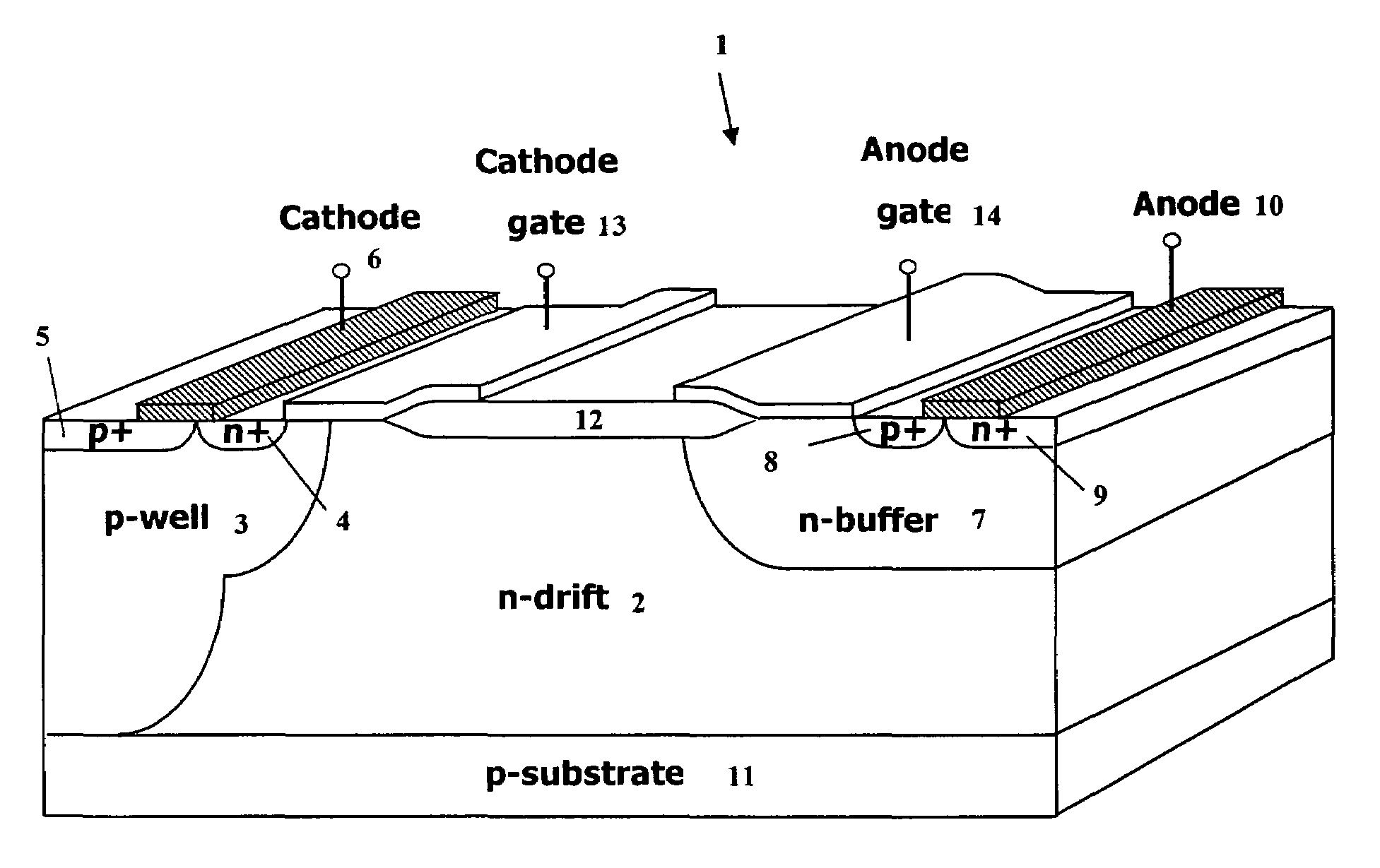
[0063]Referring now to the drawings, FIG. 1 shows schematically a perspective view of a first example of a high voltage / power lateral insulated gate bipolar transistor (LIGBT) device 1 according to an embodiment of the present invention. This example uses junction isolation technology, which is known per se. The device 1 has an n-drift region 2 having first and second ends.

[0064]At the first end of the drift region 2 there is a p-well region 3 which is adjacent to an n+ cathode region 4. In this example, the n+ cathode region 4 is formed in the p-well 3. In this example, a p+ region 5 is also formed in the p-well 3 on the opposite side of the n+ cathode region 4 to the n-drift region 2. A low voltage, “cathode” terminal 6 is in electrical contact with at least a part of the n+ cathode region 4 and, in this example, is also in electrical contact with at least a part of the p+ region 5.

[0065]At the second end of the drift region 2 is an n-buffer region or well 7 which is adjacent to a...


PUM


Abstract

A bipolar high voltage/power semiconductor device has a drift region having adjacent its ends regions of different conductivity types respectively. High and low voltage terminals are provided. A first insulated gate terminal and a second insulated gate terminal are also provided. One or more drive circuits provide appropriate voltages to the first and second insulated gate terminals so as to allow current conduction in a first direction or in a second direction that is opposite the first direction.

Description

FIELD OF THE INVENTION[0001]The present invention relates to a semiconductor device and to a method of operating a semiconductor device.[0002]The present invention is particularly concerned with high voltage semiconductor devices which can be used in power integrated circuits and has particular application to MOS-bipolar transistors, such as lateral insulated gate bipolar transistors (LIGBTs).BACKGROUND OF THE INVENTION[0003]Power devices operated in integrated circuits typically operate with a voltage in the range 20V to 1.2 kV and typically higher than 30V or 50V or so. Power devices typically operate with a current in the range 10 mA to 50A and typically higher than 0.1A and smaller than 5 A. Such devices may also be referred to as “high voltage / power devices”. These devices are typically capable of delivering from a few mWatts to 1 Watt or even a few tens of Watts of power. Their application may range from domestic appliances, electric cars, motor control, and power supplies to ...

Claims


Application Information

Patent Timeline
IPC IPC(8): H01L27/082H01L23/58H01L27/102H01L29/70H01L29/76H01L29/94H01L31/062H01L31/11H01L31/113H01L31/119
CPCH01L29/0657H01L29/0696H01L29/4232H01L29/7393H01L29/7394H01L2924/0002H01L2924/00
Inventor UDREA, FLORINUDUGAMPOLA, NISHADAMARATUNGA, GEHAN A. J.
Owner POWER INTEGRATIONS INC
Why Eureka
Try Eureka