Optoelectronic tweezers for microparticle and cell manipulation

a cell and microparticle technology, applied in the field of cell and microparticle manipulation, can solve the problems of inability to achieve high resolution and high throughput of conventional manipulation techniques, optical tweezers, electrokinetic forces (electrophoresis, dielectrophoresis, etc., to achieve high throughput and resolution. high

Active Publication Date: 2009-11-03
RGT UNIV OF CALIFORNIA
View PDF7 Cites 216 Cited by
  • Summary
  • Abstract
  • Description
  • Claims
  • Application Information

AI Technical Summary

Benefits of technology

[0013]The present invention is directed to performing particle and cell manipulation using optical image-driven light induced dielectrophoresis (DEP). The term “particle” will be used herein to reference microparticles, nanoparticles, cells, and other organic and inorganic material having a diameter generally between a few nanometers up to the order of approximately 100 μm. The techniques allow for the use of moderate intensity incoherent light sources, which create dynamic patterns that can be controlled in response to image detection and processing of actual particle composition and position.
[0014]In accordance with one embodiment of the invention, an optical image-driven dielectrophoresis apparatus and method is described for patterning electric fields on a photoconductive surface for manipulating single particles, or collections of particles. A wide variety of light sources can be utilized, such as incoherent light, and single or multistage manipulation of particles can be readily achieved.
[0018]Another embodiment provides for the manipulation of live red and white blood cells with optoelectronic tweezers. Optically-induced dielectrophoresis is enabled within the optoelectronic tweezers (OET) to manipulate live mammalian cells demonstrated by concentrating bovine red blood cells in solution. A spatial light modulator and an incoherent light source integrated in combination with the OET provide the ability to easily create reconfigurable, complex manipulation patterns. This capability is also demonstrated in the patterning of human white blood cells into complex patterns.
[0031]The first surface and second surface preferably form a continuous film upon which DEP manipulation is performed in response to images received from the optical projector. In this way lithographic patterning with conductive electrodes is not necessary for performing DEP manipulation.
[0050]Another aspect of the invention allows for an optoelectric tweezers device (OET) in which tight optical focusing is not required thereby allowing manipulation over a maximum area on the order of one square millimeter (1 mm2), or larger up to, such as 1.3 mm×1.0 mm which is many orders of magnitude larger than that which is achievable using conventional optical tweezers.
[0074]Another aspect of the invention is an OET device in which the use of low-intensity lighting allows for manipulating biological objects without loss of viability from photodamage (“opticution”) which arises when using conventional optical tweezers.

Problems solved by technology

However, conventional manipulation techniques, including optical tweezers, electrokinetic forces (electrophoresis, dielectrophoresis (DEP), traveling-wave dielectrophoresis), magnetic tweezers, acoustic traps, and hydrodynamic flows, cannot simultaneously achieve high resolution and high throughput.
However, the TWD cannot resolve individual particles.
The need of on-chip IC increases the cost of the chip, making it less attractive for disposable applications.
The trap density (i.e., approximately 400 sites / mm2) is also limited by the size of the control circuits.
Consequently, the use of electrokinetic forces and similar mechanisms provide high throughput, but lack the flexibility or the spatial resolution for controlling individual cells, or groups of cells.
In addition, these techniques require structures formed through numerous lithographic steps.
Optical tweezers, however, offer high resolution for trapping single particles, yet provide limited manipulation area due to tight focusing requirements.
These techniques require intense calculation for creating even simple optical patterns.

Method used


Image

  • Optoelectronic tweezers for microparticle and cell manipulation
  • Optoelectronic tweezers for microparticle and cell manipulation
  • Optoelectronic tweezers for microparticle and cell manipulation

Examples


embodiment 90

[0184]FIG. 11 illustrates an embodiment 90 of the optoelectronic tweezers device with a liquid buffer containing the particles of interest between the upper ITO glass layer and the lower photoconductive layer. To separate the top and bottom layers, 100 μm thick spacers (not shown) are utilized.

[0185]In demonstrating the OET device and methods herein the digital micromirror device (DMD) in a light projector was used to image the virtual electrodes. An embodiment of the optoelectronic tweezers device was formed by evaporating a 10 nm thick aluminum film onto a glass substrate to provide electrical contact. A 1 μm thick undoped amorphous silicon (a-Si) photoconductive layer was then deposited, for example by utilizing plasma-enhanced chemical vapor deposition. It should be appreciated that detailed fine-pitched features need not be created on the first and second retention layers, wherein detailed lithographic steps are not necessary. To protect the photoconductive film, a 20 nm thick ...

embodiment 100

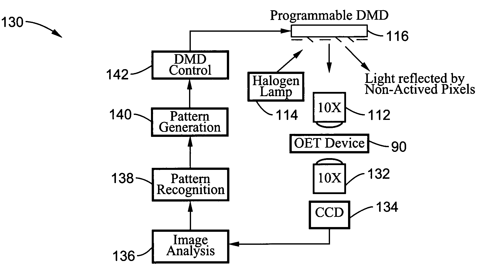
[0190]FIG. 12 illustrates, by way of example, a optical setup embodiment 100 for this OET demonstration. Observation of the particles under test is performed preferably utilizing a microscopic imaging system 120, for example a Nikon TE2000U inverted microscope. A CCD camera attached to the observation port of the microscope recorded images and video of these demonstrations and tests. To produce the electric field necessary for DEP, an AC voltage of approximately 10VPP at 100 kHz (i.e., Agilent® 33120A) was applied across the top ITO surface and the bottom photoconductive surface of the OET device.

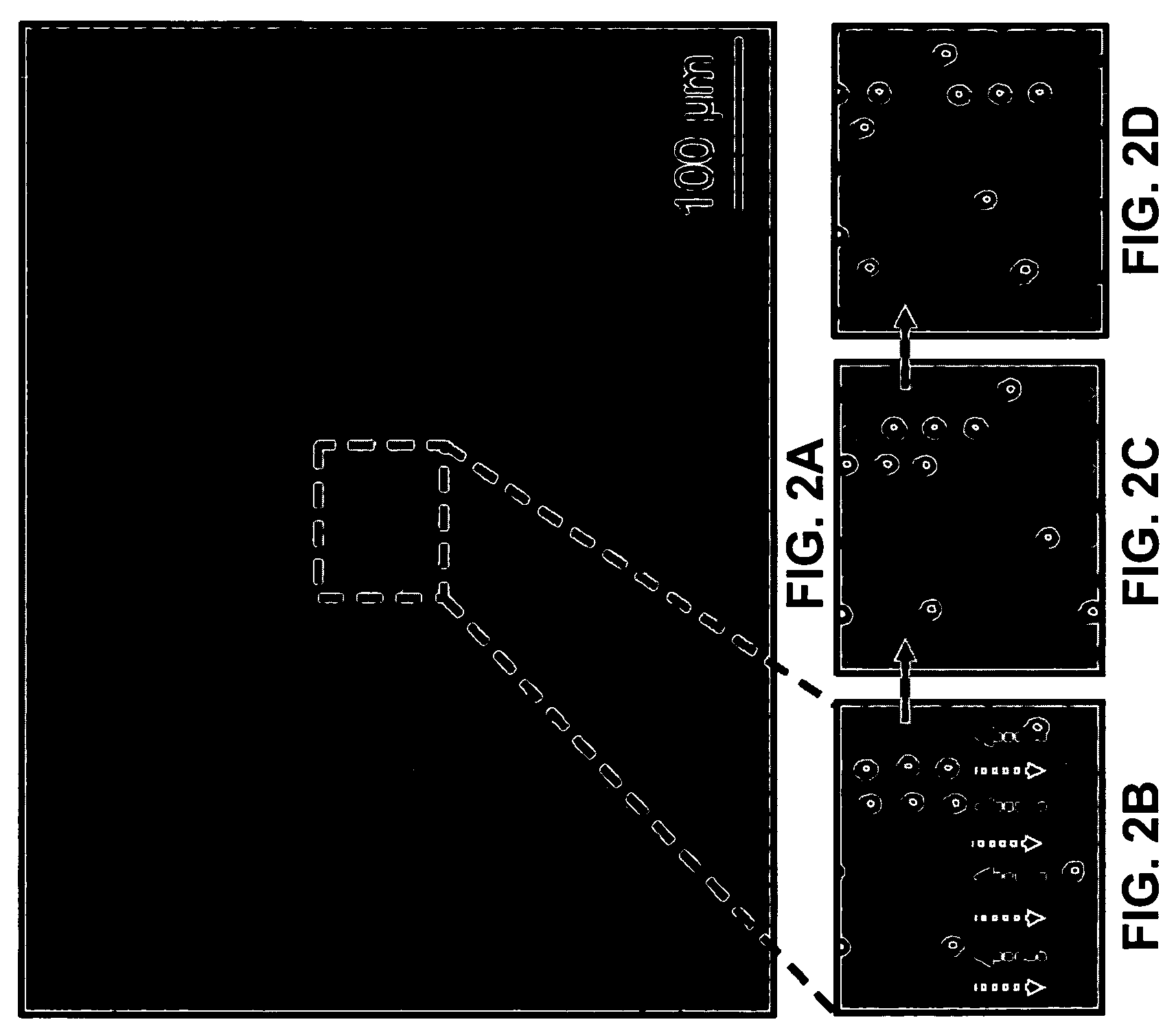
[0191]FIGS. 13A-13B illustrate self-organization of 45 μm polystyrene spheres into an array configuration. After the initial grid illumination shown in FIG. 13A, the randomly arranged particles move towards the dark areas via negative DEP. After five seconds, all particles are contained within the array cells as shown in FIG. 13B.

[0192]The self-organization of randomly distributed 45 kHz po...

embodiment 210

[0249]FIGS. 27A-27B illustrate an OET embodiment 210 in FIG. 27A with an Illustration of the light induced dielectrophoresis mechanism in FIG. 27B.

[0250]The term Re[K*(ω)] can have any value between 1 to −½, depending on the applied AC frequency and the polarizability of the particle and the medium. If Re[K*(ω)]<0, it is called negative DEP with the direction of the DEP force towards lower electric field. Since the DEP force is proportional to the gradient of the square of the applied electric field, a highly non-uniform electric field is desired to achieve a higher trapping force. In the following experiment a light induced negative DEP force is demonstrated.

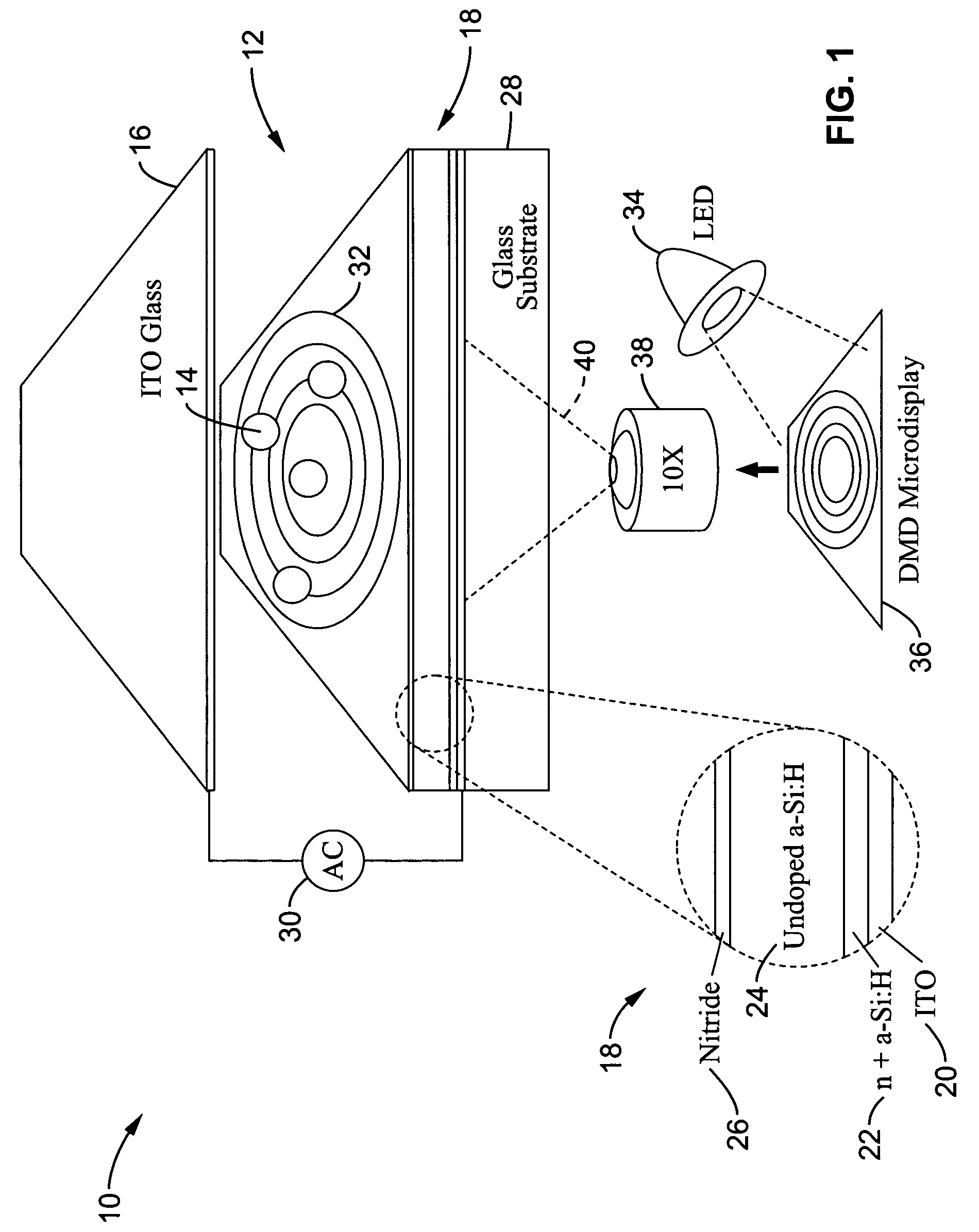
[0251]In FIG. 27A, the structure of the optoelectronic tweezers are shown with a liquid solution 12 containing the particles sandwiched between two surfaces separated by a gap spacing of 100 μm. The top surface 16 is a commercial ITO glass. The bottom surface is a glass substrate 28 coated with three pattern-less layers: a 2000...


PUM

PropertyMeasurementUnit
diameteraaaaaaaaaa
optical actuating poweraaaaaaaaaa
diametersaaaaaaaaaa

Abstract

An optical image-driven light induced dielectrophoresis (DEP) apparatus and method are described which provide for the manipulation of particles or cells with a diameter on the order of 100 μm or less. The apparatus is referred to as optoelectric tweezers (OET) and provides a number of advantages over conventional optical tweezers, in particular the ability to perform operations in parallel and over a large area without damage to living cells. The OET device generally comprises a planar liquid-filled structure having one or more portions which are photoconductive to convert incoming light to a change in the electric field pattern. The light patterns are dynamically generated to provide a number of manipulation structures that can manipulate single particles and cells or groups of particles / cells. The OET preferably includes a microscopic imaging means to provide feedback for the optical manipulation, such as detecting position and characteristics wherein the light patterns are modulated accordingly.

Description

CROSS-REFERENCE TO RELATED APPLICATIONS[0001]This application claims priority from U.S. provisional application Ser. No. 60 / 561,587 filed on Apr. 12, 2004, incorporated herein by reference in its entirety.STATEMENT REGARDING FEDERALLY SPONSORED RESEARCH OR DEVELOPMENT[0002]This invention was made with Government support under Grant No. 442521-WM-22622 / NCC2-1364, awarded by NASA. The Government has certain rights in this invention.INCORPORATION-BY-REFERENCE OF MATERIAL SUBMITTED ON A COMPACT DISC[0003]Not ApplicableNOTICE OF MATERIAL SUBJECT TO COPYRIGHT PROTECTION[0004]A portion of the material in this patent document is subject to copyright protection under the copyright laws of the United States and of other countries. The owner of the copyright rights has no objection to the facsimile reproduction by anyone of the patent document or the patent disclosure, as it appears in the United States Patent and Trademark Office publicly available file or records, but otherwise reserves all ...

Claims


Application Information

Patent Timeline
Patent Type & Authority Patents(United States)
IPC IPC(8): G01N21/86G01V8/00C12M3/04
CPCB03C5/026G01N2035/1046B01L3/502761B01L2400/0454
Inventor WU, MING CHIANGCHIOU, PEI YUOHTA, AARON T.
Owner RGT UNIV OF CALIFORNIA
Why Eureka
Try Eureka