Elevated source and drain elements for strained-channel heterojuntion field-effect transistors

Inactive Publication Date: 2009-11-10
TAIWAN SEMICON MFG CO LTD
View PDF310 Cites 12 Cited by
  • Summary
  • Abstract
  • Description
  • Claims
  • Application Information

AI Technical Summary

Benefits of technology

[0003]An elevated source/drain process enables the formation of good contacts to source and drain regions of a FET formed in a strained channel, such as strained silicon. In an embodiment, a bottommost boundary of the metal-semiconductor alloy contact extends into the strained silicon portion of each of the source and drain regions. The metal-semiconductor alloy contact does not exten

Problems solved by technology

This strain increases carrier mobilities, thereby lowering the sheet resistance of the semiconductor layer.
This strain also results in a

Method used


Image

  • Elevated source and drain elements for strained-channel heterojuntion field-effect transistors
  • Elevated source and drain elements for strained-channel heterojuntion field-effect transistors
  • Elevated source and drain elements for strained-channel heterojuntion field-effect transistors

Examples


Embodiment Construction

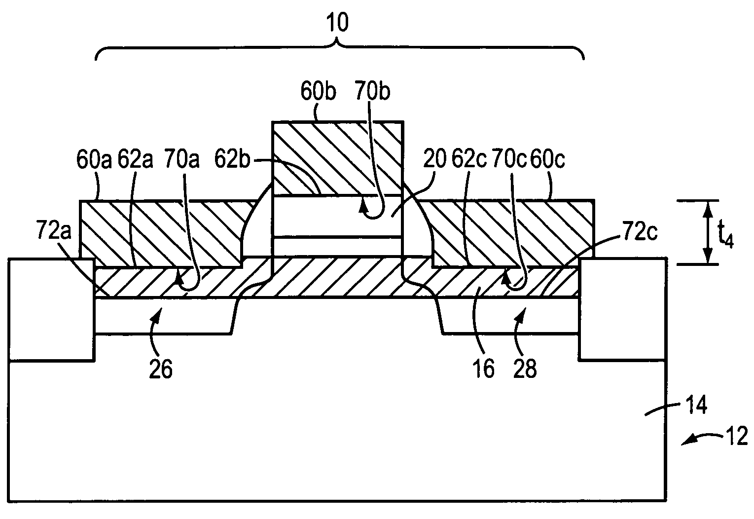
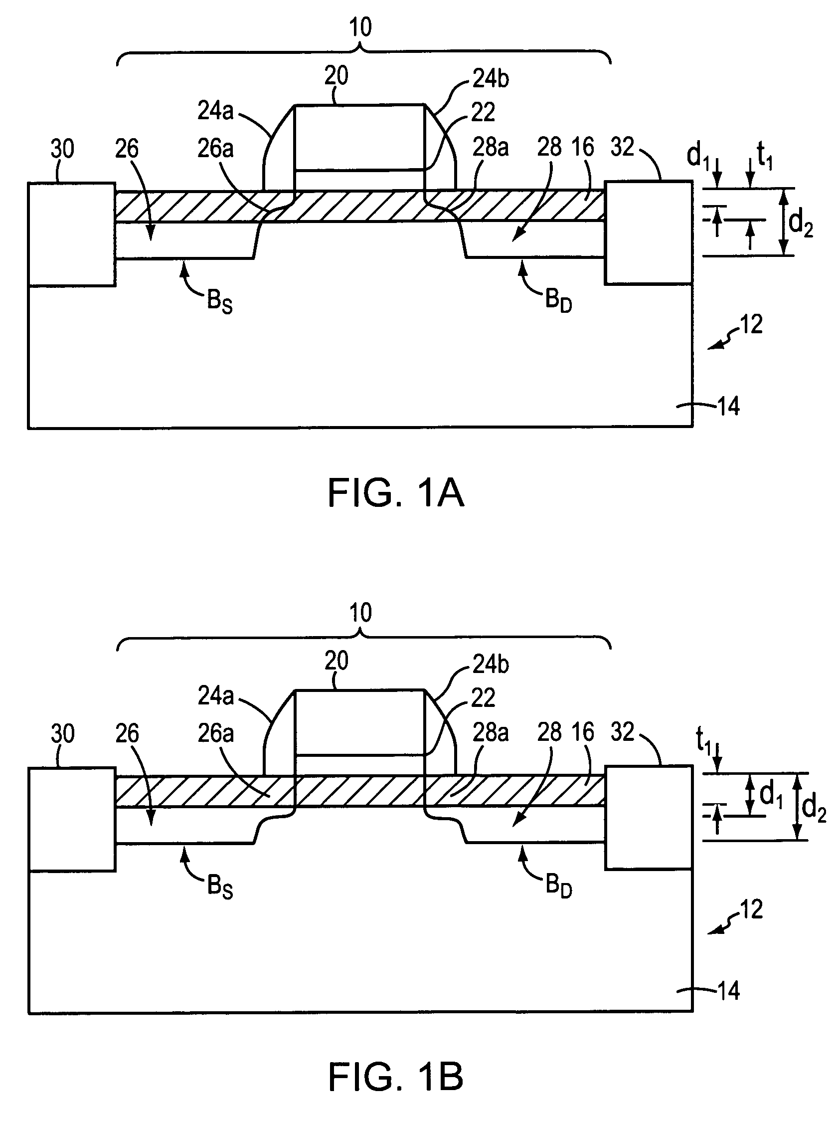
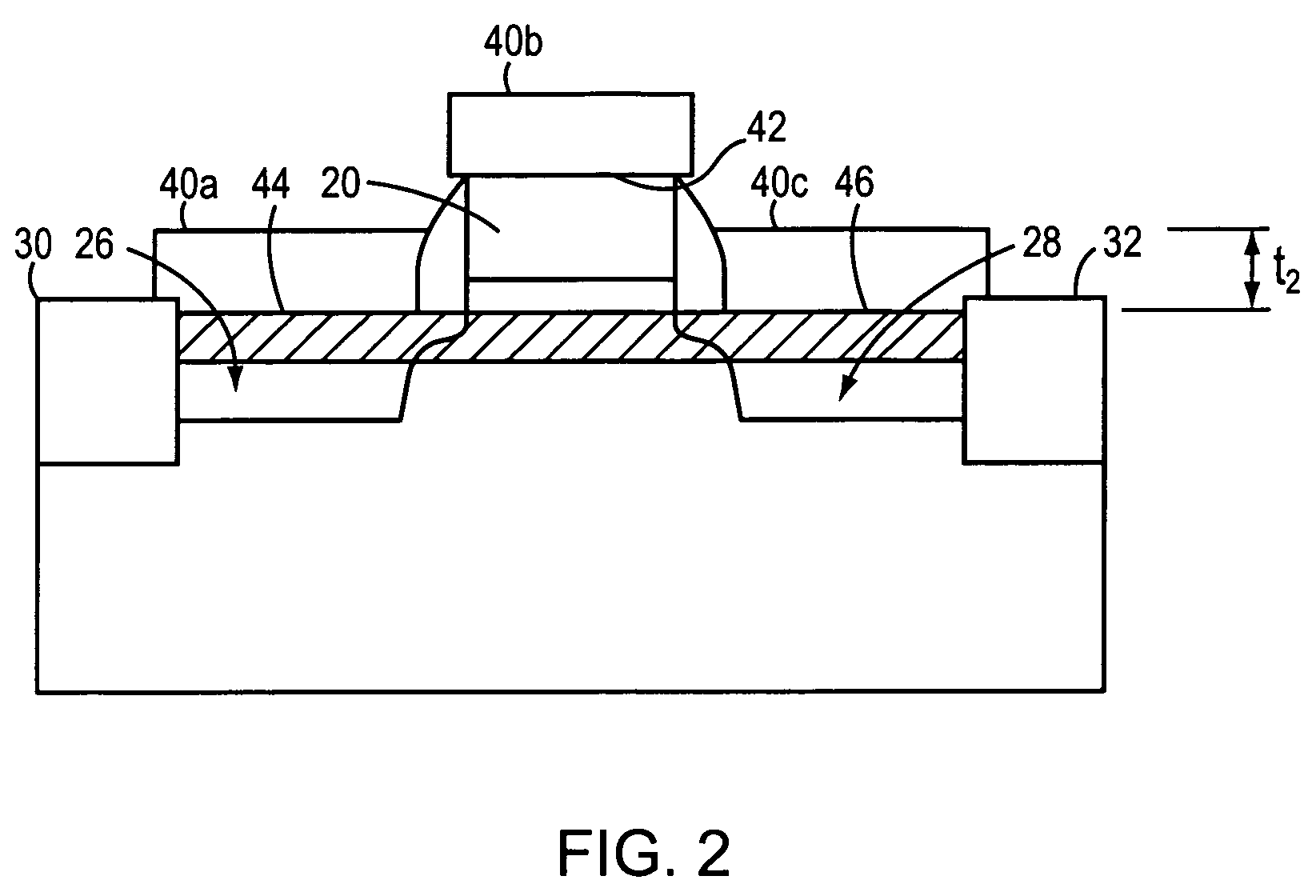
[0019]Referring to FIGS. 1a and 1b, a transistor 10 is formed on a substrate 12. Substrate 12 includes a relaxed layer 14, which has a lattice constant greater than that of silicon. Underlying layer 14 includes, for example, Si0.80Ge0.20 and has a lattice constant of 5.472 Å. Substrate 12 also has a surface layer 16, disposed over relaxed layer 14. Surface layer 16 includes strained silicon, has a thickness t1 of, e.g., 200 Å, and has a low resistivity of, e.g., less then approximately 0.001 ohm-cm. A suitable substrate 12 with relaxed layer 14 and surface layer 16 can be readily obtained from, e.g., IQE Silicon Compounds, Ltd., UK.

[0020]Transistor 10 includes a gate 20 disposed over a gate dielectric 22. Gate 20 can be formed by, for example, depositing and patterning polysilicon, and gate dielectric 22 can be formed by, for example, growth of a gate oxide, such as silicon dioxide. A first and a second sidewall spacer 24a, 24b are formed proximate gate 20. Sidewall spacers 24a, 24b...


PUM


Abstract

A semiconductor structure having a surface layer disposed over a substrate, the surface layer including strained silicon. A contact layer is disposed over a portion of the surface layer, the contact layer including a metal-semiconductor alloy. A bottommost boundary of the contact layer is disposed above a bottommost boundary of the surface layer.

Description

FIELD OF THE INVENTION[0001]This invention generally pertains to semiconductor structures formed on strained layers.BACKGROUND[0002]Field-effect transistors (FETs) based on strained heterojunction channels have shown significant promise for increased drive current and higher frequency operation, in comparison to traditional FETs with relaxed silicon channels. Strained heterojunction channels are fabricated from materials such as silicon (Si), silicon-germanium (SiGe), germanium (Ge), etc. Forming high-quality electrical contacts is difficult when the source and drain regions of a FET include materials other than pure silicon. High quality contacts to silicon-based FETs are traditionally achieved through a silicide process, where a metal such as cobalt or titanium is alloyed with silicon to form the contact. This process is typically not as effective with semiconductor materials other than silicon. For example, a cobalt silicide contact formed to a source disposed in a strained Si la...

Claims


Application Information

Patent Timeline
IPC IPC(8): H01L27/088H01L29/45H01L21/336H01L29/10H01L29/80
CPCH01L29/1054H01L29/665H01L29/802H01L29/66628H01L29/6659
Inventor LOCHTEFELD, ANTHONY J.LANGDO, THOMAS A.WESTHOFF, RICHARD
Owner TAIWAN SEMICON MFG CO LTD
Why Eureka
Try Eureka