Methods for forming multilayer structures

a multi-layer structure and structure technology, applied in the direction of variable capacitors, fixed capacitor details, fixed capacitors, etc., can solve the problems of limited dielectric constant of the dielectric layer, limited capability of the final capacitor, and problems in regard to certain electrical properties

Active Publication Date: 2009-11-24
DUPONT ELECTRONICS INC
View PDF31 Cites 27 Cited by
  • Summary
  • Abstract
  • Description
  • Claims
  • Application Information

AI Technical Summary

Problems solved by technology

Various types of dielectric layers are currently being used in the processing of circuit board capacitors, however, the dielectric constant of the dielectric layer is limited and problems exist in regard to certain electrical properties, such as low dielectric withstanding voltage and high leakage current.
Both of these problems limit the capability of the final capacitor and, in many cases, limit the ability to decrease the thickness of the dielectric layer within the capacitor to the desired level.
Further, the requirement for solder joints reduces reliability and increases costs of fabrication.

Method used

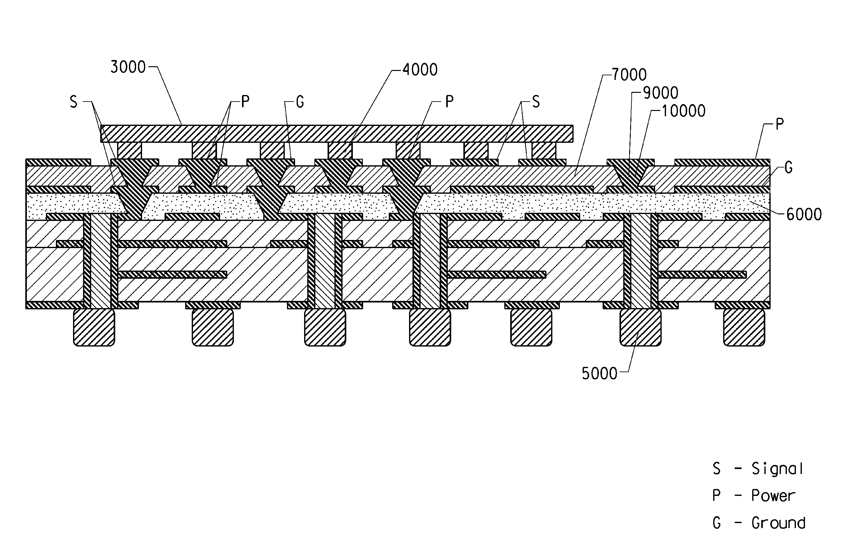
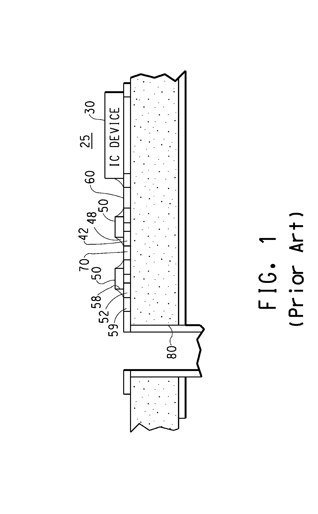
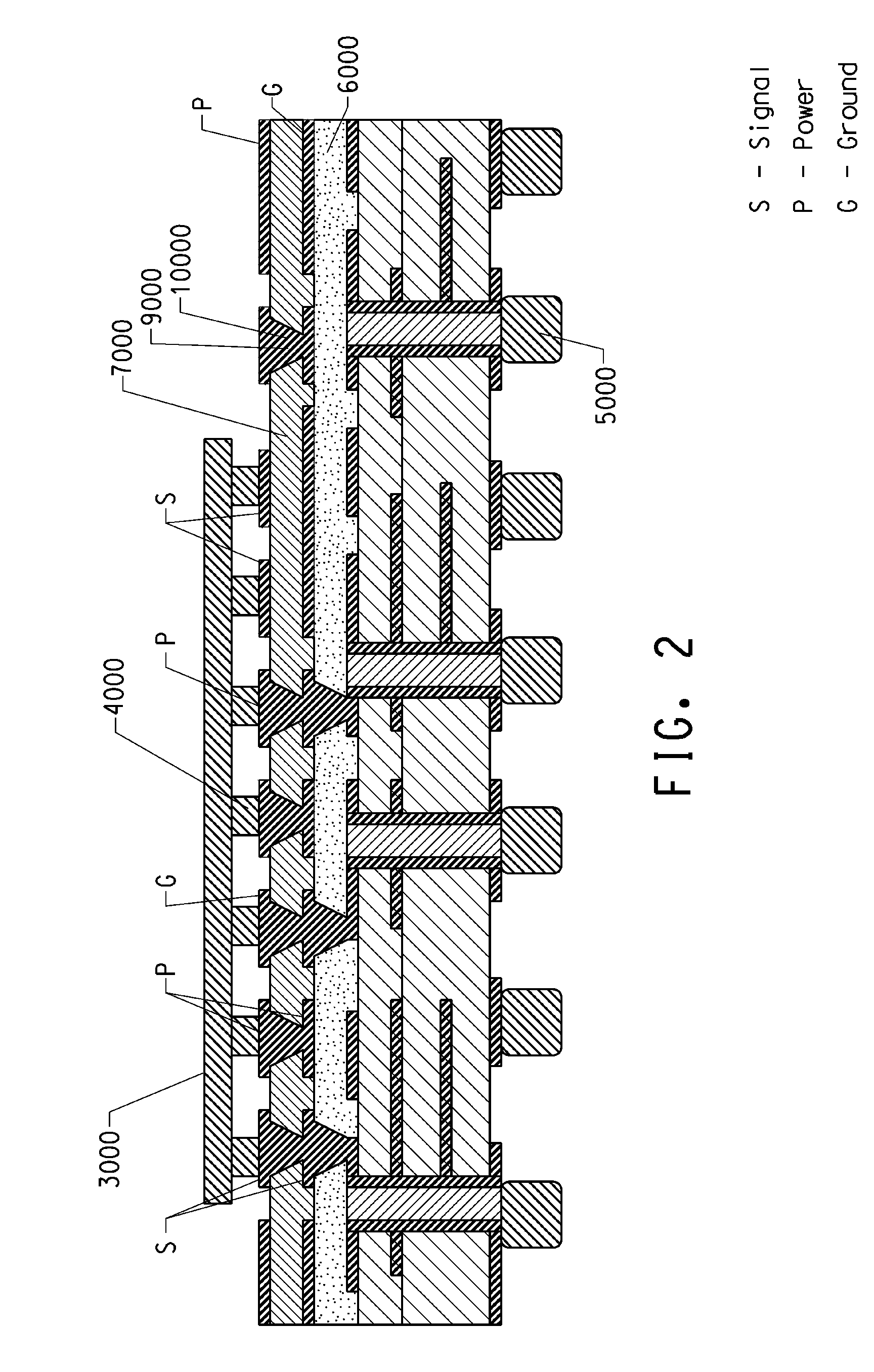

Image

  • Methods for forming multilayer structures
  • Methods for forming multilayer structures
  • Methods for forming multilayer structures

Examples


examples

Preparation of TiO2-filled Dielectric Film

[0044]First, 30 g of DuPont Ti-Pure® R-101 titanium dioxide powder were dispersed in a high shear mixer into a solution of DriClad® epoxy-based resin in MEK (methyle ethyle ketone) solvent (source: EIT-Endicott Interconnect Technologies). The weight of the solution was 211 g containing 160 g resin (75.8% solids). 2-methylimidazole (0.208 g) was dissolved in 90 g MEK and added to the dispersion (imidazole to resin weight ratio of 0.13 / 100). The resulting dispersion had a viscosity of 19 cps and a 55.83% solids content. The dispersion was then board-coated on an about 25 micron thick Mylar® foil using a 150 micron board coating blade. The dried coating thickness was approximately 40 micron; the coating width was about 18 cm, and the coating length was about 137 cm. The coating was dried with a hot air blower. The coating was then covered with a silicone-release Mylar® foil so that the rolled up coated foil would not stick to itself. The coated...

example # 1

Example #1

[0048]A solution of 160 grams of a polyamic acid derived from the following monomers: pyromellitic dianhydride (PMDA), 4,4′-oxydiphthalic anydride (ODPA) and 1,3-bis-(4-aminophenoxy) benzene (APB-134) was mixed with 120 grams of Dimethylacetamide (DMAC) solvent and 30 grams of DuPont Ti-Pure® R-101 titanium dioxide powder. This solution was stirred in a high speed mixer until the powder was dispersed. Small amounts of additional monomer were added until a viscosity of 500 poise was reached. This solution was then coated on solid surface as a uniform coating. The coating was then dried at 170° C. to remove about 70 to 80% of the solvent. The formed film was then removed from the solid surface. This film was then cured in an oven at 350° C. for 1 hour. The final film thickness was 1.1 mils and the filler loading was 26 volume percent.

[0049]The cured titanium dioxide filled film was then laminated between two sheets of copper foil. Each copper sheet was 36 microns thick. The ...

example # 2

Example #2

[0051]A solution of 18 lbs of DMAC and 18 lbs of DuPont Ti-Pure® R-101 titanium dioxide powder was stirred for 1 hour in a high speed mixer. Then 84 lbs of a polyamic acid derived from the following monomers: pyromellitic dianhydride (PMDA), 4,4′-oxydiphthalic anydride (ODPA) and 1,3-bis-(4-aminophenoxy) benzene (APB-134) was added. This mixture was stirred for an additional 30 minutes. Small amounts of additional monomer were added until a viscosity of 400 poise was reached.

[0052]This solution was then cast on to a continued sheet of copper foil (36 microns thick). The solution was dried at 190° C. to about 90% solids. The coated copper was then cured in an oven at 350° C. for 1 hour. The final film thicknesses were 8 and 12 microns. The filler loading was 29 volume percent.

[0053]The filled polyimide film coated on copper was then laminated to a sheet of copper foil. The copper sheet was 35 microns thick. The lamination used an autoclave under vacuum with maximum laminati...


PUM

PropertyMeasurementUnit
dielectric constantaaaaaaaaaa
volume percentaaaaaaaaaa
particle sizeaaaaaaaaaa

Abstract

The present invention relates to methods of forming multilayer structures and the structures themselves. In one embodiment, a method of forming a multilayer structure comprises: providing a dielectric composition comprising paraelectric filler and polymer wherein the paraelectric filler has a dielectric constant between 50 and 150; applying the dielectric composition to a carrier film thus forming a multilayer film comprising a dielectric layer and carrier film layer; laminating the multilayer film to a circuitized core wherein the dielectric layer of the multilayer film is facing the circuitized core; and removing the carrier film layer from the dielectric layer prior to processing; applying a metallic layer to the dielectric layer wherein the circuitized core, dielectric layer and metallic layer form a planar capacitor; and processing the planar capacitor to form a multilayer structure.

Description

RELATED APPLICATIONS[0001]This application is related to and claims priority to the applications U.S. Provisional Application Ser. Nos. 60 / 638001, 60 / 637813, 60 / 637817, and 60 / 637816, respectively filed in the U.S. Patent and Trademark Office on Dec. 21, 2004.TECHNICAL FIELD[0002]The technical field relates to dielectric composition(s) and film(s) and their use in electronic circuitry and components, such as a multilayer printed circuit. The multilayer printed circuit can be a rigid, flexible, or rigid-flex circuit board, a multilayered chip package, or a multichip package.TECHNICAL BACKGROUND[0003]An increasing need exists for reducing the size and increasing the performance of integrated circuit components. One common part of the integrated circuit components, for example planar capacitor components, includes a dielectric layer that is formed from a composition comprising a dielectric functional filler material and a polymer. Typically, using a dielectric functional filler materia...

Claims


Application Information

Patent Timeline
Patent Type & Authority Patents(United States)
IPC IPC(8): H05K3/30
CPCH01L21/4857H01L23/49894H05K1/162H01L23/49822Y10T29/4913H01L2224/16H01L2924/01012H01L2924/0102H01L2924/01046H01L2924/01057H01L2924/01078H01L2924/15311H01L2924/19105H01L2924/3011H05K3/4602H05K3/4626H05K3/4688H05K2201/0209H05K2203/066H01L2924/01019H01L2924/01087H01L2224/16225H01L2224/16235Y10T29/49165Y10T29/49147Y10T29/435Y10T29/49156Y10T29/43H01G4/30
Inventor BANERJI, SOUNAKCOX, G. SIDNEYDIETZ, KARL HARTMANN
Owner DUPONT ELECTRONICS INC
Why Eureka
Try Eureka