Reactive ion etching for semiconductor device feature topography modification

a technology of reactive ions and semiconductor devices, applied in vacuum evaporation coatings, chemical vapor deposition coatings, coatings, etc., can solve the problems of increasing the aspect ratio, affecting the operation of the completed device, and progressively more difficult to fill gaps without leaving voids, etc., to achieve improved etch control, good overall gapfill capability, and precise control

Inactive Publication Date: 2009-12-08
APPLIED MATERIALS INC
View PDF68 Cites 226 Cited by
  • Summary
  • Abstract
  • Description
  • Claims
  • Application Information

AI Technical Summary

Benefits of technology

[0006]Embodiments of the invention provide for an improvement in etch control during a dep/etch/dep process by using a chemistry that allows more precise control over the both the concentration and distribution of etchant atoms in a process chamber. In addition to flowing an etchant-ion precursor, a reactive scavenging-ion pre...

Problems solved by technology

One of the persistent challenges faced in the development of semiconductor technology is the desire to increase the density of circuit elements and interconnections on substrates without introducing spurious interactions between them.
As circuit densities increase, however, the widths of these gaps decrease, increase their aspect ratios and making it progressively more difficult to fill the gaps without leaving voids.
The formation of voids when the gap is not filled completely is undesirable because they may adversely affect operation of the completed device, such as by trapping impurities within the insulative material.
The high reactivity of the species in the plasma reduces the energy required for a chemical reaction to take place, and thus lowers the temperature required for such CVD processes when compared with conventional thermal CVD processes.
Such dep/etch/dep processes have also been used with PECVD techniques, but ...

Method used


Image

  • Reactive ion etching for semiconductor device feature topography modification
  • Reactive ion etching for semiconductor device feature topography modification
  • Reactive ion etching for semiconductor device feature topography modification

Examples


Embodiment Construction

1. Introduction

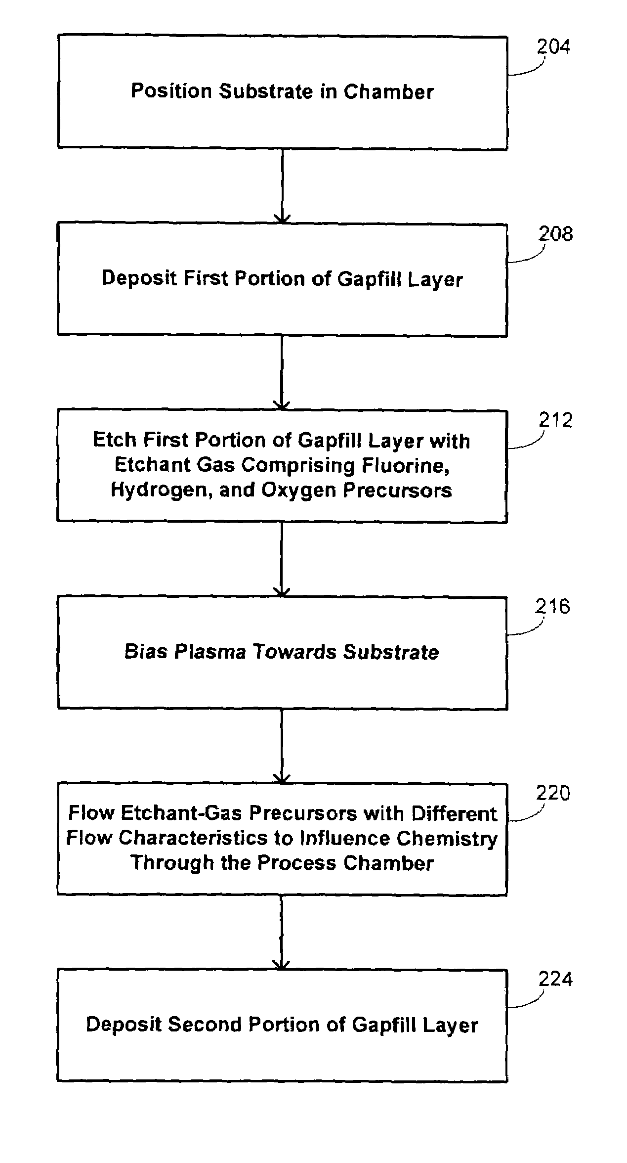
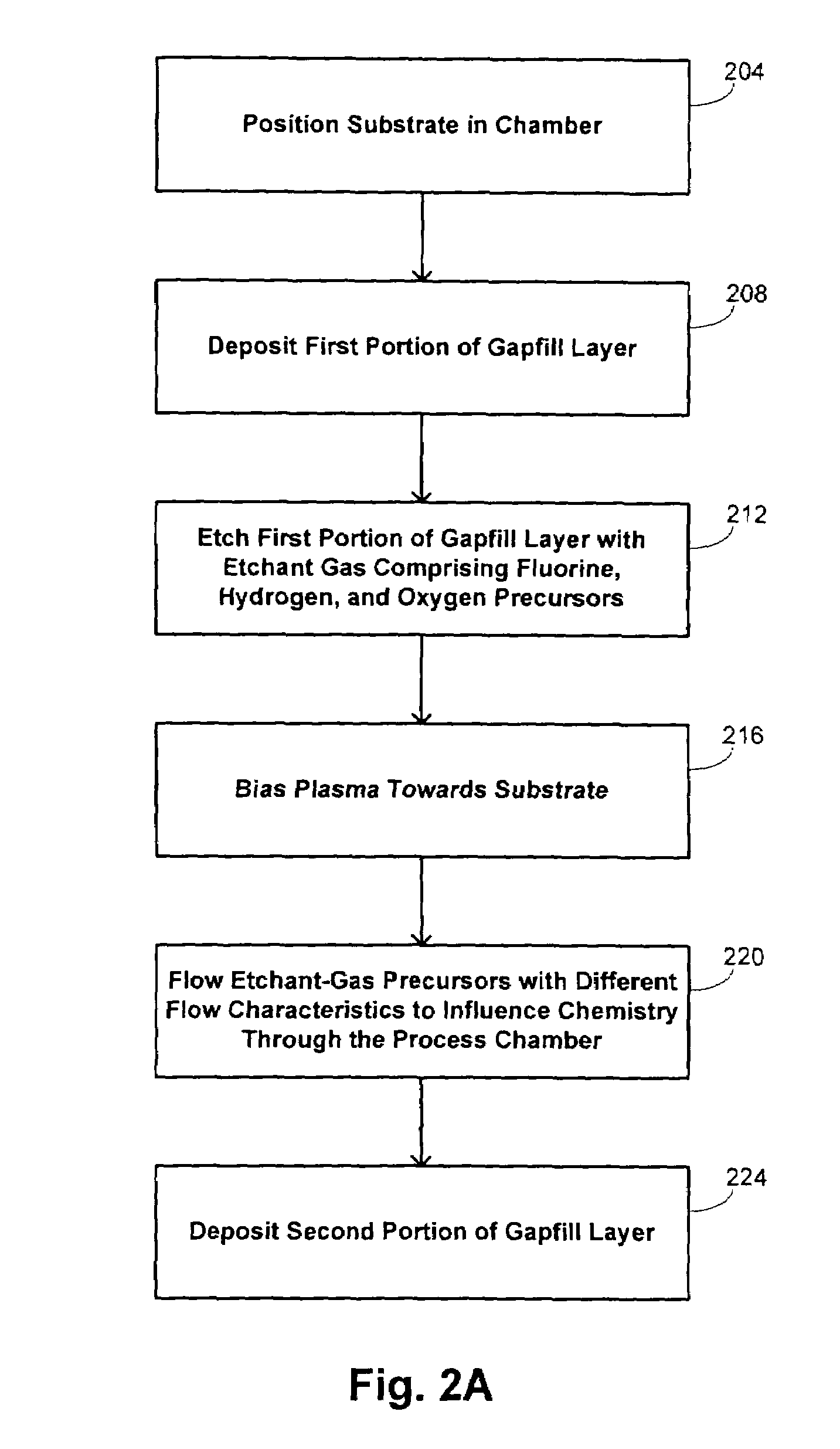
[0025]Embodiments of the invention are directed to methods and apparatus for depositing a film to fill a gap in a surface of a substrate with a multistep deposition and etching process. Films deposited according to the techniques of the invention have excellent gapfill capabilities and are able to fill high-aspect-ratio gaps encountered in, for example, shallow-trench-isolation (“STI”), intermetal-dielectric (“IMD”), and premetal-dielectric (“PMD”) structures, among others. Films deposited by the methods of the invention are suitable for use in the fabrication of a variety of integrated circuits, and are particularly useful in technology that uses minimum feature sizes of 0.06 μm or smaller.

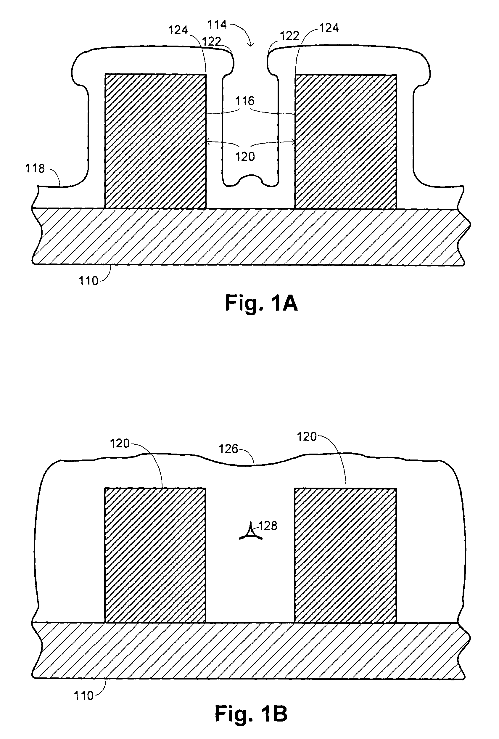
[0026]The gapfill problem addressed by embodiments of the invention is illustrated schematically with the cross-sectional views shown in FIGS. 1A and 1B. FIG. 1A shows a vertical cross section of a substrate 110, such as may be provided with a semiconductor wafer, having a layer of...


PUM

PropertyMeasurementUnit
Volumetric flow rateaaaaaaaaaa

Abstract

A film is deposited on a substrate disposed in a substrate processing chamber. The substrate has a trench formed between adjacent raised surfaces. A first portion of the film is deposited over the substrate from a first gaseous mixture flowed into the process chamber by chemical-vapor deposition. Thereafter, the first portion is etched by flowing an etchant gas having a halogen precursor, a hydrogen precursor, and an oxygen precursor into the process chamber. Thereafter, a second portion of the film is deposited over the substrate from a second gaseous mixture flowed into the processing chamber by chemical-vapor deposition.

Description

CROSS REFERENCE TO RELATED APPLICATION[0001]This application is a continuation-in-part application of U.S. patent application Ser. No. 10 / 279,961, entitled “HIGH DENSITY PLASMA CVD PROCESS FOR GAPFILL INTO HIGH ASPECT RATIO FEATURES,” filed Oct. 23, 2002 by Farhan Ahmad et al., the entire disclosure of which is incorporated herein by reference for all purposes.BACKGROUND OF THE INVENTION[0002]One of the persistent challenges faced in the development of semiconductor technology is the desire to increase the density of circuit elements and interconnections on substrates without introducing spurious interactions between them. Unwanted interactions are typically prevented by providing gaps or trenches that are filled with electrically insulative material to isolate the elements both physically and electrically. As circuit densities increase, however, the widths of these gaps decrease, increase their aspect ratios and making it progressively more difficult to fill the gaps without leavin...

Claims


Application Information

Patent Timeline
IPC IPC(8): C23C14/35C23C16/00H01L21/311C23C16/04C23C16/40C23C16/505H01L21/316
CPCC23C16/045C23C16/401C23C16/505H01L21/02129H01L21/31633H01L21/02164H01L21/02274H01L21/31612H01L21/31625H01L21/02131
Inventor MUNGEKAR, HEMANT P.PATEL, ANJANA M.VELLAIKAL, MANOJWANG, ANCHUANKAPOOR, BIKRAM
Owner APPLIED MATERIALS INC
Why Eureka
Try Eureka