

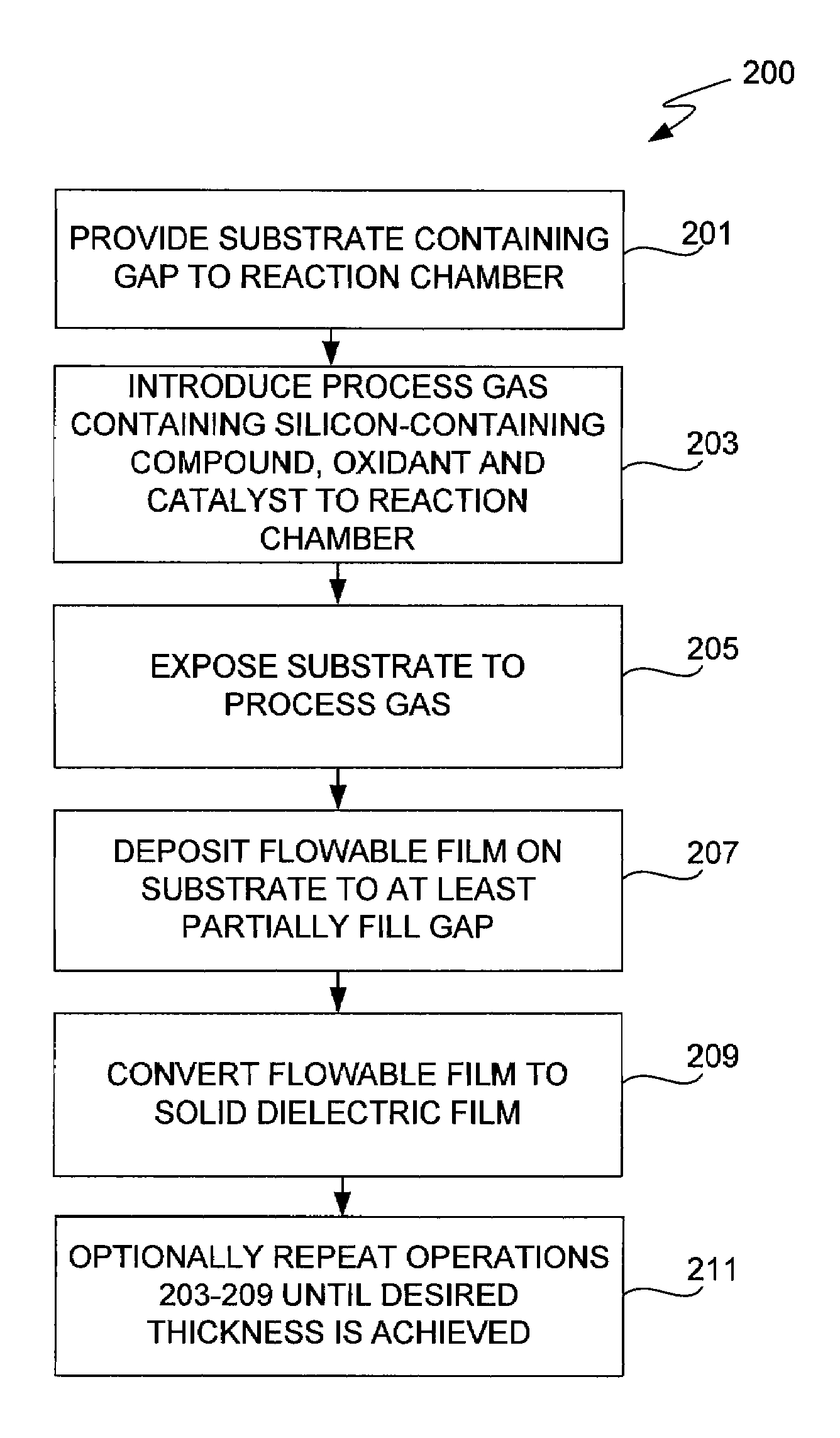
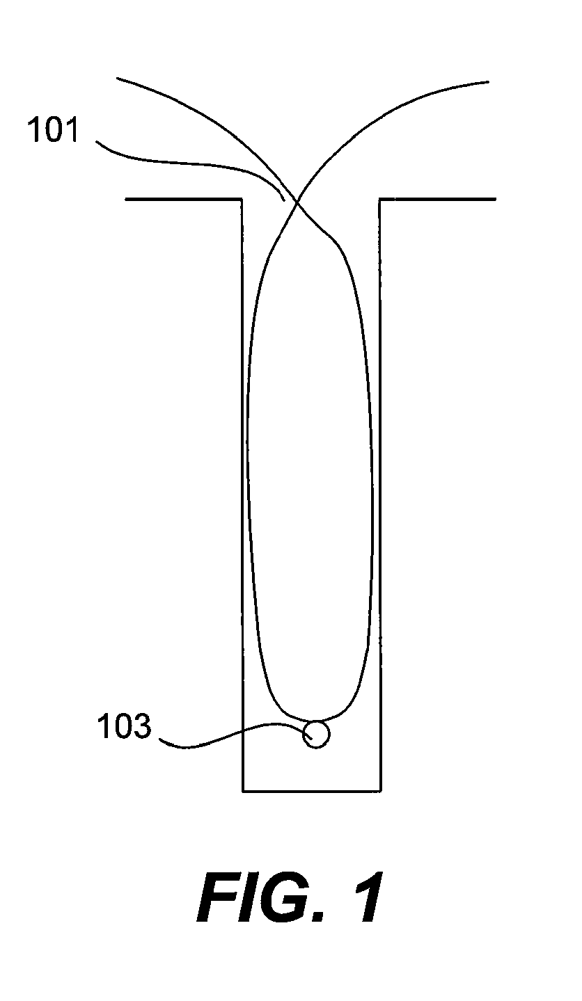
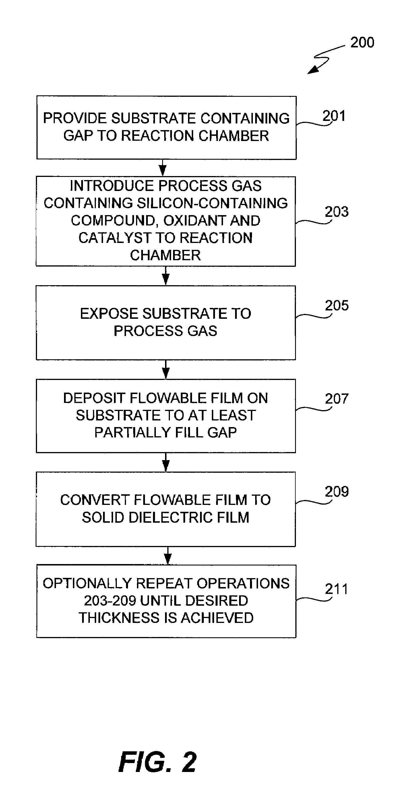
CVD flowable gap fill
a flowable gap and filling technology, applied in the direction of semiconductor/solid-state device manufacturing, basic electric elements, electric apparatus, etc., can solve the problems of void-free filling or uniform lining without significant necking of high aspect ratio spaces (e.g., ar>3:1), and the top part of a high aspect ratio structure sometimes closes
- Summary
- Abstract
- Description
- Claims
- Application Information
AI Technical Summary
Benefits of technology
Problems solved by technology
Method used
Image

Examples
example 1
Effect of Using Cl− Catalyst
[0075]Wafers were exposed to trimethoxysilane (TriMOS) gas and steam at the following conditions:
[0076]
ABCatalyst Content00.4%Cl(provided as (CH3O)2Si(H)Cl)TriMOS flow rate1.3mL / min1.3mL / minSteam flow rate0.13mL / min0.13mL / minPressure4-50torr4-50torrTemperature8C.8C.Exposure Time20-60sec20-60sec
The wafer was allowed to cool to 8° C. with a constant flow of He at 2 SLM before exposing to steam (1.00 mL / min) over a period of 10 s. The wafer is then exposed to TriMOS (1.30 mL / min) and steam (0.13 mL / min) for a period of 45 s during which time the He-carrier gas was flowing at 2 SLM. Pressures were varied during the process.
[0077]No deposition was observed for “A.” For “B,” full, continuous-color wafer coverage of film was observed. Film thickness was observed to be fairly uniform, with most of the wafer having about 100 nm of film.
example 2
Effect of Thermal Cure Budget on Film Structure
[0078]FIG. 6 shows FTIR spectra of dielectric films formed by deposition of flowable films and subsequent thermal cure. Spectra of films cured at 600 C, 800 C, 850 C and 900 C for 60 min are shown. Si—H and cage-like Si—O peaks are indicated on the figure. As can be seen, a small Si—H peak is present at 600 C. Higher temperatures (at or above about 850 C) lead to a complete conversion of Si—H to Si—O. The higher temperature cure also leads to transformation of the cage-like Si—O to branch-like structures, which results in a thermal oxide like films.
example 3
Multi-Stage Anneal
[0079]A single stage 60 min anneal (600 C in air) was compared to multi-stage (60 min / 600 C in air followed by 900 C vacuum) anneal. The film resulting from the multi-stage cure was observed to be more etch resistant towards 6:1 BOE (buffered HF etching) solution. In general, the denser the film is, the lower the film wet etch rate (WER) is. Typically, a small wafer with the film is immersed in the 6:1 BOE solution for a period of 10 seconds. The differences in film thickness (measured by any available Opti-probe or ellipsometry techniques) divided by the wet etch time (10 sec) provides the wet etch rate (WER) of a given film in the 6:1 BOE solution. A small piece of the single stage cured (600° C. in air) film subjected to immersion in 6:1 BOE for 10s exhibited a WER of 306 nm / min whereas the multi-stage cured sample (600° C. in air followed by 900° C. in vacuum) exhibited a much slower WER of 230 nm / min film. This indicates that the multi-stage anneal results in ...
PUM
 Abstract
Description
Claims
Application Information