
Photovoltaic structure with a conductive nanowire array electrode

a photovoltaic structure and array electrode technology, applied in nanoinformatics, pv power plants, solid-state devices, etc., can solve the problems of inconvenient control, inconvenient control, and high cost of single-crystal cells, so as to achieve easy control

Inactive Publication Date: 2009-12-22
SHARP KK
View PDF26 Cites 32 Cited by
  • Summary
  • Abstract
  • Description
  • Claims
  • Application Information

AI Technical Summary

Benefits of technology

This patent describes a method for making a photovoltaic structure using conductive nanowires. The method involves forming a bottom electrode with the nanowires, then sequentially adding layers of semiconductor material to the nanowires. The top electrode is then added to complete the structure. The use of conductive nanowires makes the process easier to control, and the method can be used with a variety of semiconductor materials. The technical effect is the improved efficiency and ease of production of photovoltaic structures using conductive nanowires.

Problems solved by technology

Efficiency is a known problem associated with solar cells.
Single-crystal cells have an efficiency on the order of 14-20%, and are expensive, because they are cut from cylindrical ingots.
While cheaper and more easily formed into desired shapes, these cells are less efficient.
Nanocrystalline structures are inefficient, but easier to make.
However, organic solar cells suffer from degradation upon exposure to UV light and have limited lifetimes.
While these cells are cheaper to make than Si or inorganic cells, their efficiencies are low and sensitivity to the environment is high.
The problem with this kind of structure is the disordered nanostructures, in that the two phases created are separated by too large of a length scale.
Consequently, some of the generated excitons are not able to diffuse to an interface to be dissociated before they decay.
Unfortunately this structure is very hard to make and is not commercially feasible.
Sometimes the formation temperature of the semiconductor array is high, preventing the use of the process with cheap glass or plastic substrates.
Thus, it is difficult to grow a semiconductor nanowire or nanorod array overlying a flat-surface electrode.

Method used


Image

  • Photovoltaic structure with a conductive nanowire array electrode
  • Photovoltaic structure with a conductive nanowire array electrode
  • Photovoltaic structure with a conductive nanowire array electrode

Examples


Embodiment Construction

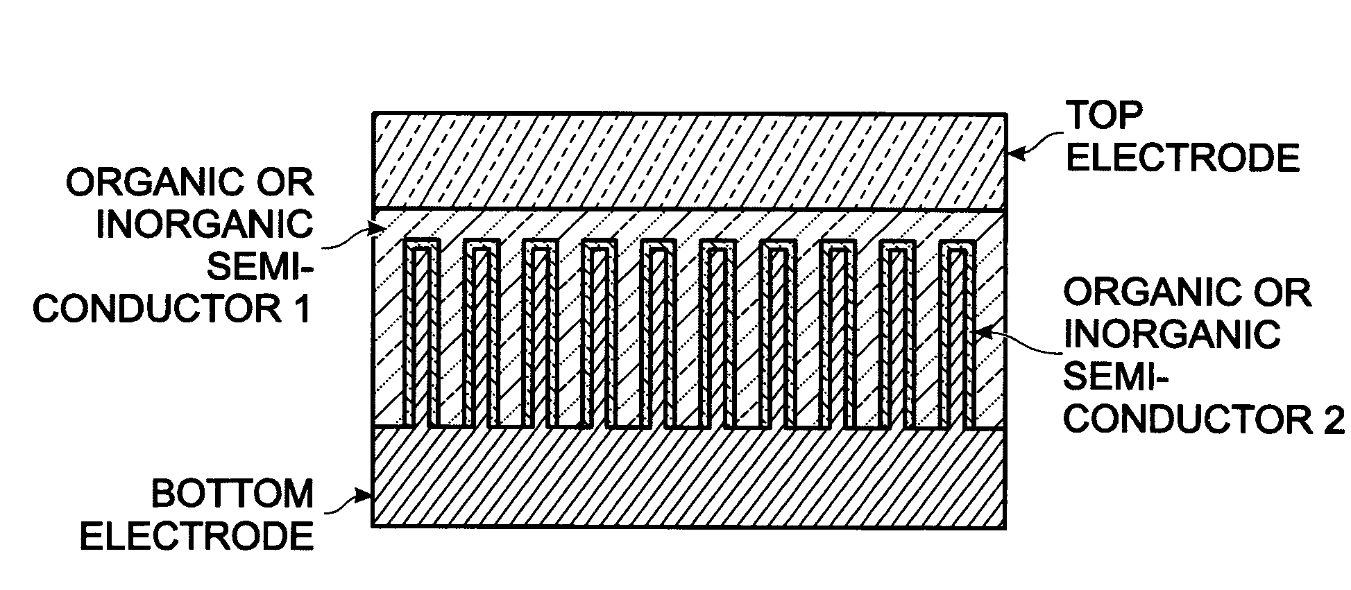
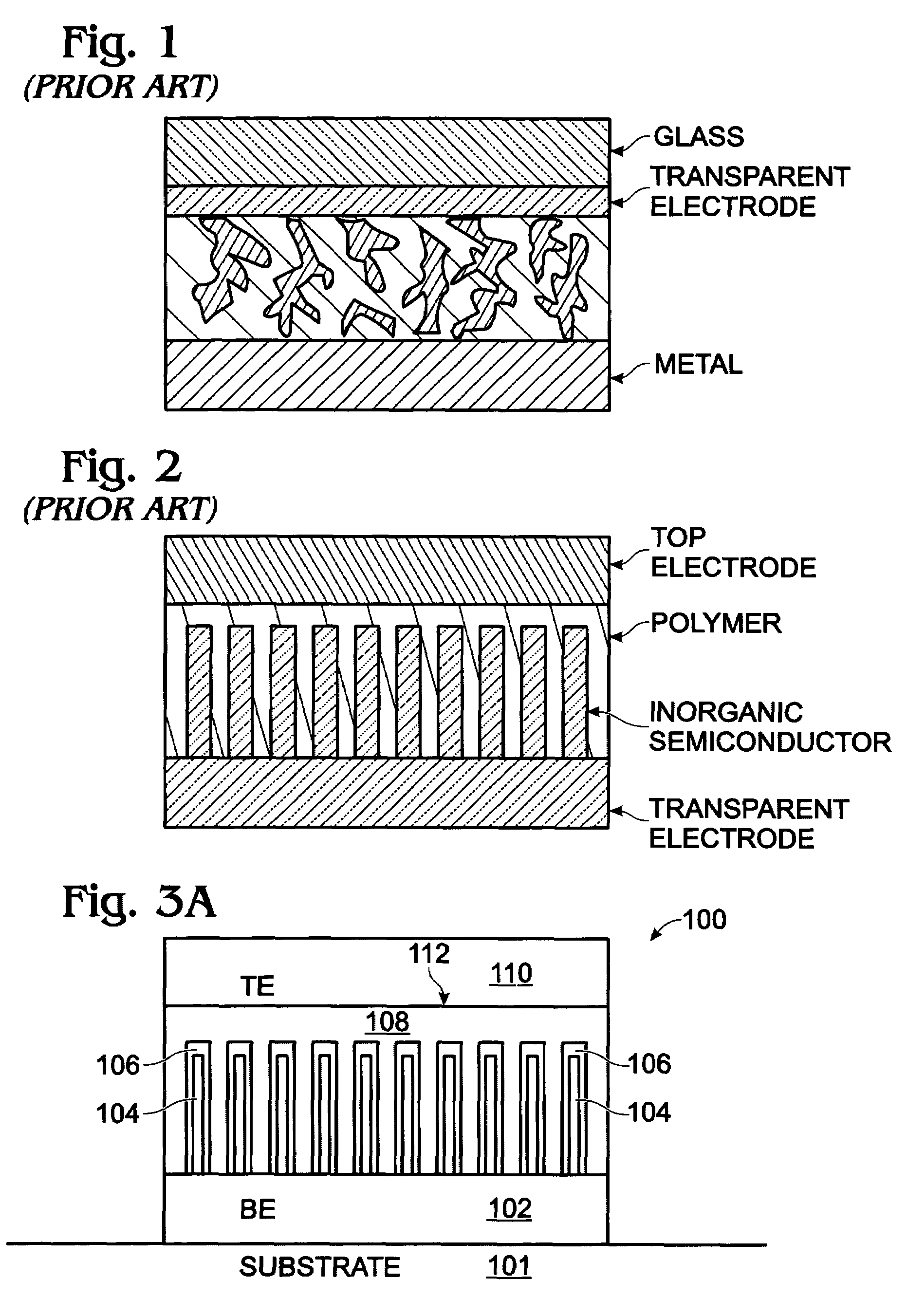
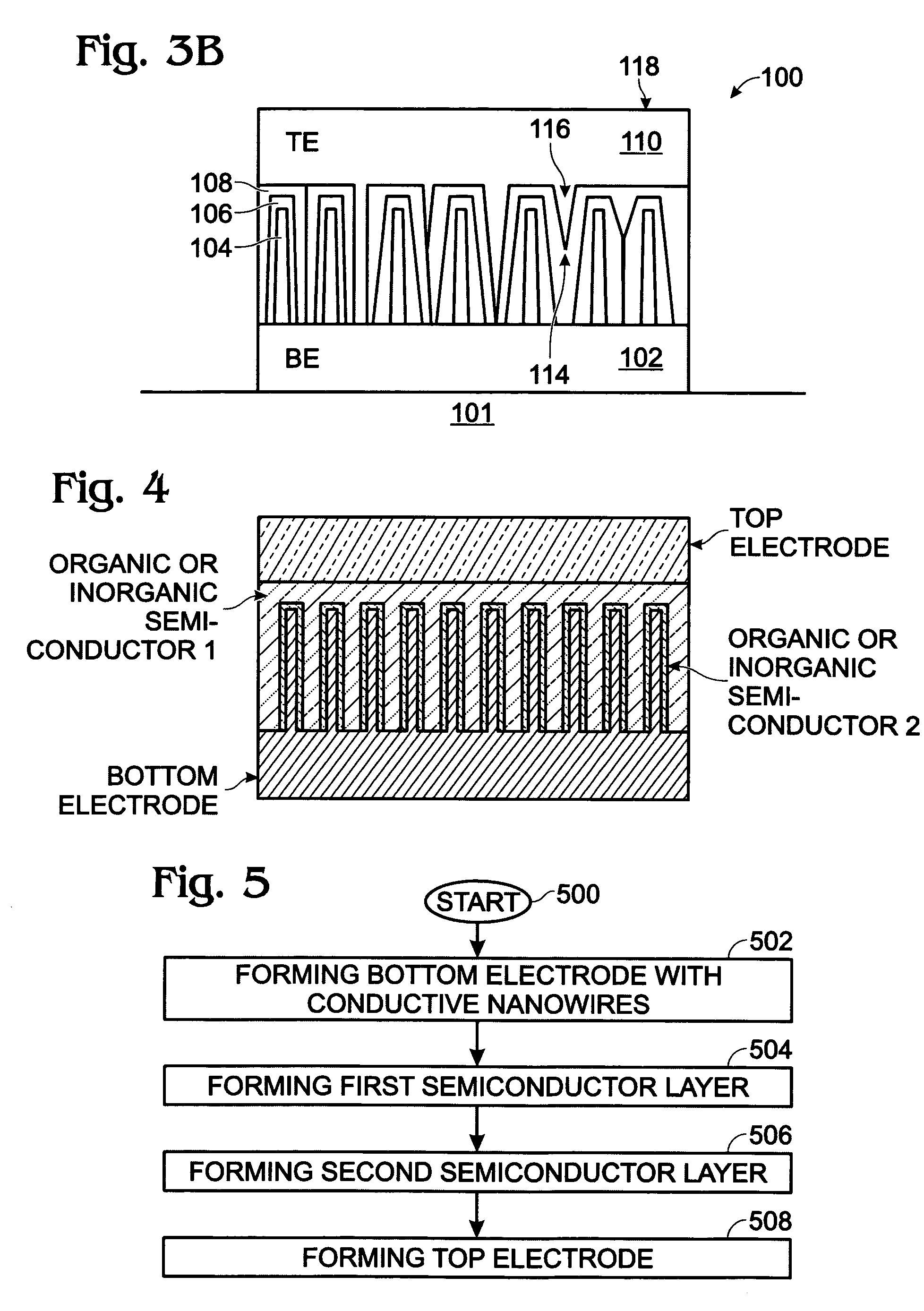
[0029]FIGS. 3A and 3B are partial cross-sectional views of a photovoltaic (PV) structure with a conductive nanowire array electrode. The PV structure 100 comprises a bottom electrode (BE) 102 with conductive nanowires 104. In some aspects, the bottom electrode is formed on a substrate such as a semiconductor material, glass, ceramic, metal, quartz, or plastic. The nanowires 104 are typically a material such as IrO2, In2O3, SnO2, carbon nanotube (CNT), or ITO. However, other conductive materials may also be used. The nanowire may alternately be called a nanorod, nanotube, or nanofiber. The nanowire is not limited to any particular diameter, length, or density. The nanowire may be single or multi-walled. A first semiconductor layer 106 of a first dopant type overlies the nanowires 104. A second semiconductor layer 108 of a second dopant type, opposite of the first dopant type, overlies the first semiconductor layer 106. A top electrode (TE) 110 overlies the second semiconductor layer ...


PUM


Abstract

A photovoltaic (PV) structure is provided, along with a method for forming a PV structure with a conductive nanowire array electrode. The method comprises: forming a bottom electrode with conductive nanowires; forming a first semiconductor layer of a first dopant type (i.e., n-type) overlying the nanowires; forming a second semiconductor layer of a second dopant type, opposite of the first dopant type (i.e., p-type), overlying the first semiconductor layer; and, forming a top electrode overlying the second semiconductor layer. The first and second semiconductor layers can be a material such as a conductive polymer, a conjugated polymer with a fullerene derivative, and inorganic materials such as CdSe, CdS, Titania, or ZnO. The conductive nanowires can be a material such as IrO2, In2O3, SnO2, or indium tin oxide (ITO).

Description

BACKGROUND OF THE INVENTION[0001]1. Field of the Invention[0002]This invention generally relates to integrated circuit (IC) and solar cell fabrication and, more particularly, to a photovoltaic device using a conductive nanowire array electrode.[0003]2. Description of the Related Art[0004]A photovoltaic (PV) cell, which is often referred to as a solar cell, is most often a semiconductor device with a large-area p-n junction diode. In the presence of sunlight, the PV is capable of generating electrical energy. This conversion is called the photovoltaic effect. Efficiency is a known problem associated with solar cells. Efficiency is the ratio of the electric power output to the light power input. Solar radiation has an approximate maximum value of 1000 watts per square-meter (W / m2). Solar cell efficiencies vary between 6%, using amorphous silicon materials, and 30% or even higher efficiencies, using experimental materials.[0005]The most common solar cell material is crystalline silicon...

Claims


Application Information

Patent Timeline
Patent Type & Authority Patents(United States)
IPC IPC(8): H01L21/00
CPCB82Y10/00H01L51/4213H01L51/4233H01L51/441H01L51/4226H01L51/0046H01L51/0048Y02E10/549Y02E10/543Y02E10/52H10K85/211H10K85/221H10K30/152H10K30/151H10K30/81H10K30/50H10K30/352H10K30/10
Inventor ZHANG, FENGYANBARROWCLIFF, ROBERT A.HSU, SHENG TENG
Owner SHARP KK
Learn More