Method and apparatus for controlling dopant concentration during BPSG film deposition to reduce nitride consumption

a technology of bpsg film and concentration, applied in the direction of resistive material coating, liquid/solution decomposition chemical coating, superimposed coating process, etc., can solve the problems of defective device formation, inconsistent processing, etc., and achieve the effect of reducing the consumption of nitrid

Inactive Publication Date: 2009-12-29
APPLIED MATERIALS INC
View PDF19 Cites 7 Cited by
  • Summary
  • Abstract
  • Description
  • Claims
  • Application Information

AI Technical Summary

Benefits of technology

[0009]A method and apparatus for controlling dopant concentration during borophosphosilicate glass film deposition on a semiconductor wafer to reduce consumption of nitride on the semiconductor wafer are described. In one embodiment of the invention, the method starts by placing a substrate having a nitride layer in a reaction chamber and providing a silicon source, an

Problems solved by technology

Inconsistent dopant concentration, particularly at interfaces with other ma

Method used


Image

  • Method and apparatus for controlling dopant concentration during BPSG film deposition to reduce nitride consumption
  • Method and apparatus for controlling dopant concentration during BPSG film deposition to reduce nitride consumption
  • Method and apparatus for controlling dopant concentration during BPSG film deposition to reduce nitride consumption

Examples


Embodiment Construction

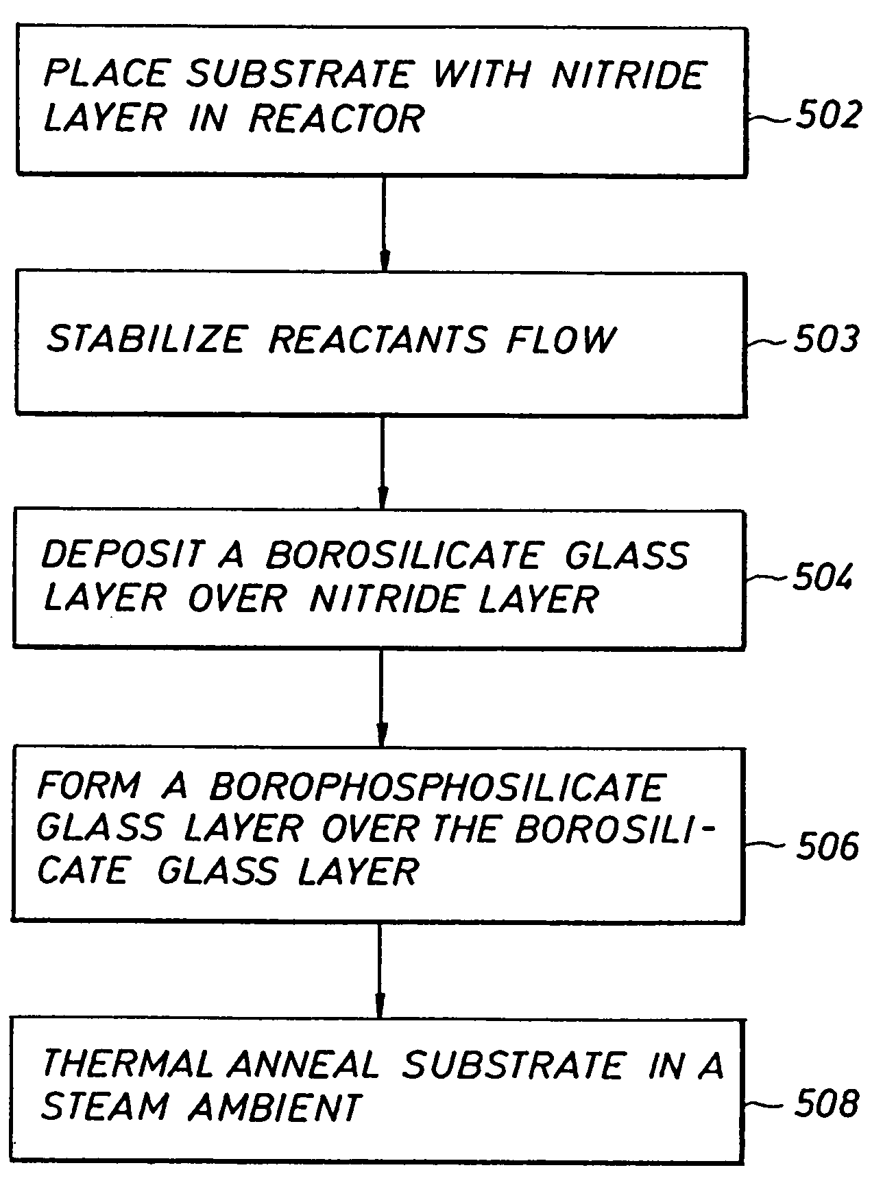
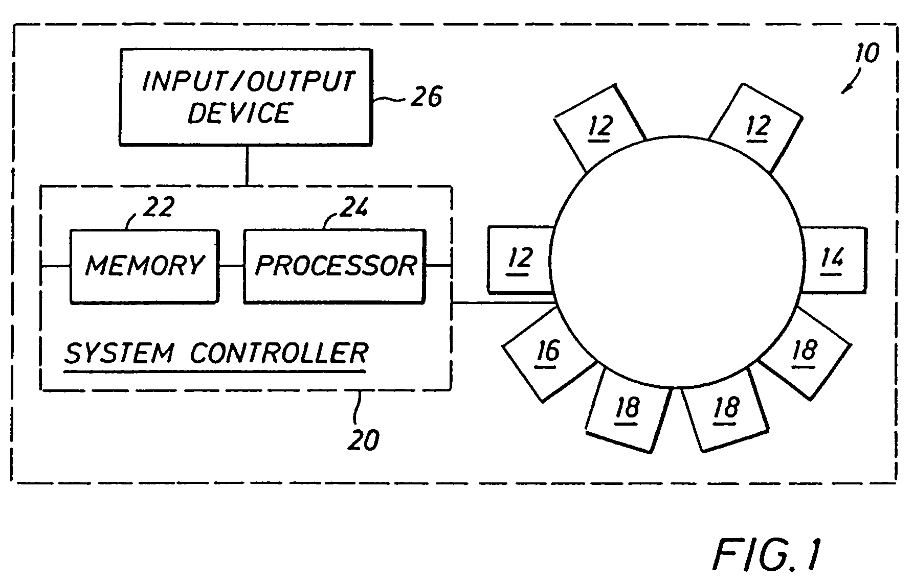
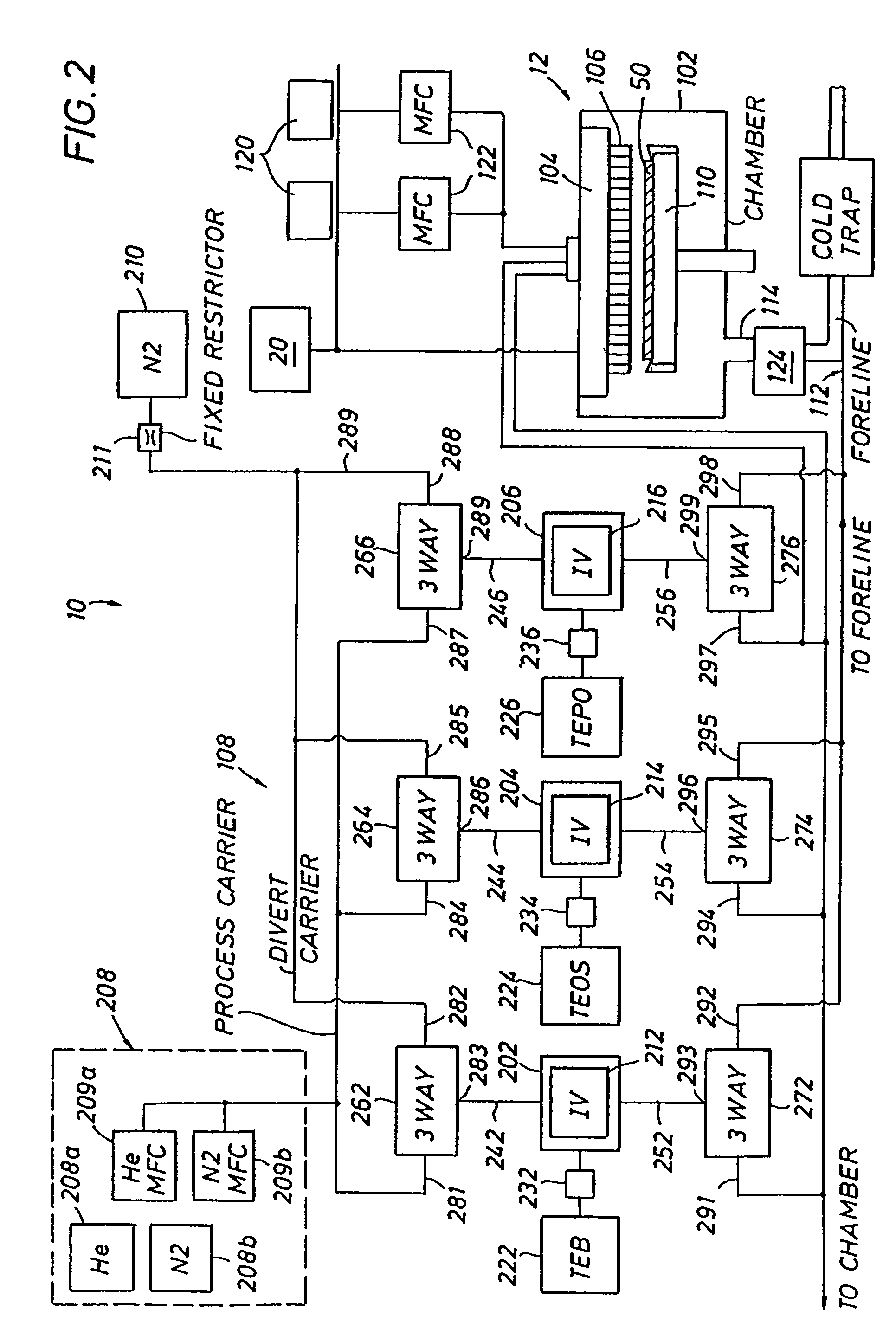
[0018]The present invention describes a novel method and apparatus for reducing the nitride consumption during integrated circuit manufacture. In the following detailed description numerous specific details such as apparatus configurations as well as process specifics such as time and temperature are set forth in order to provide a thorough understanding of the present invention. One skilled in the art will appreciate the ability to use alternative configuration and process details to the disclosed specifics without parting from the scope of the present invention. In other instances, well-known semiconductor processing equipment and techniques have not been described in detail in order to not unnecessarily obscure the present invention.

[0019]The present invention describes a novel method and apparatus for selectively controlling dopant concentration during borophosphosilicate glass film deposition on a semiconductor wafer to reduce nitride consumption. According to the present inven...


PUM

PropertyMeasurementUnit
Timeaaaaaaaaaa
Percent by massaaaaaaaaaa
Concentrationaaaaaaaaaa

Abstract

A method and apparatus for controlling dopant concentration during borophosphosilicate glass film deposition on a semiconductor wafer to reduce consumption of nitride on the semiconductor wafer. In one embodiment of the invention, the method starts by placing a substrate having a nitride layer in a reaction chamber and providing a silicon source, an oxygen source and a boron source into the reaction chamber while delaying providing a phosphorous source into the reaction chamber to form a borosilicate glass layer over the nitride layer. The method continues by providing the silicon, oxygen, boron and phosphorous sources into the reaction chamber to form a borophosphosilicate film over the borosilicate glass layer.

Description

BACKGROUND OF THE INVENTION[0001]1. Field of the Invention[0002]The present invention relates generally to the filed of substrate processing for semiconductor manufacturing and more specifically to an improved method for controlling dopant concentration during borophosphosilicate glass (BPSG) film deposition on a semiconductor wafer to reduce consumption of nitride layer on the semiconductor wafer.[0003]2. Description of Related Art[0004]Silicon oxide is widely used as an insulating layer in the manufacture of semiconductor devices. For a number of years, boron and phosphorous doped silicate films, such as borophosphosilicate glass (BPSG) films, deposited with liquid sources such as tetraethylorthosilicate (TEOS), have gained preference among silicon oxide films for their superior gap filling capability upon glass reflow.[0005]BPSG films are generally deposited on a silicon wafer or substrate by thermal or plasma enhanced chemical vapor deposition (CVD) processes from a reaction of ...

Claims


Application Information

Patent Timeline
IPC IPC(8): C23C16/22C23C16/00H01L21/31C23C16/40H01L21/316
CPCC23C16/401H01L21/02129H01L21/022H01L21/31625H01L21/02304H01L21/02337H01L21/02271C23C16/40
Inventor MUKAI, KEVINCHANDRAN, SHANKAR
Owner APPLIED MATERIALS INC
Why Eureka
Try Eureka