Check patentability & draft patents in minutes with Patsnap Eureka AI!

CCD color solid-state image pickup device

a solid-state image and pickup device technology, applied in the direction of television system scanning details, radio control devices, television systems, etc., can solve the problems of color filtering, inability to effectively utilize all wavelength components, image photographed and reproduced by a solid-state image pickup device using color filters of complementary color systems is usually inferior in quality to that photographed and reproduced, etc., to prevent the occurrence of incident light loss, improve color reproducibility and image quality, and enhance sensitivity and resolution

Inactive Publication Date: 2010-02-02
FUJIFILM CORP
View PDF20 Cites 8 Cited by
  • Summary
  • Abstract
  • Description
  • Claims
  • Application Information

AI Technical Summary

Benefits of technology

[0023]By means of such a configuration, signal electric charges corresponding to incident light of different colors are stored in respective electric charge storage layers of one light-receiving section without use of color filters. Hence, incident light can be effectively utilized without placing a squeeze on the area of the light-receiving region and while lessening or eliminating moiré, a false signal, and a false color.
[0024]In the CCD color solid-state image pickup device of the invention, an electric charge path, which causes electric charges stored in the electric charge storage layers to migrate to the surface of the semiconductor substrate and is formed from a heavily-doped impurity region, may be provided in an electric charge storage layer from among the plurality of electric charge storage layers, the electric charge storage-layer being provided in the semiconductor substrate. By means of such a configuration, reading of signal electric charges from the respective electric charge storage layers is facilitated.
[0025]In the CCD color solid-state image pickup device of the invention, a concentration gradient may be imparted such that the dopant concentration of the electric charge storage layers formed as heavily-doped impurity regions and the dopant concentration of the electric charge path continually connected to the electric charge storage layer increase as the electric charge storage layer and the electric charge path approach the vertical transfer path. By means of such a configuration, reading of signal electric charges stored in the storage sections is facilitated, thereby preventing retention of unread signal electric charges.
[0031]In the CCD color solid-state image pickup device of the present invention, on-chip light gathering optical systems may be provided on upper portions of the respective light-receiving sections, and one opening of each light-shielding film may correspond to one of the light-receiving sections. By means of this configuration, even when the substantial area of the light-receiving section is enlarged to become double or triple, an essentially identical resolution is obtained for a given size of a CCD. Therefore, when an attempt is made to miniaturize the image pickup device or increase the number of pixels, information about all color components (R, G, and B) can be obtained independently from one pixel even under the same design rule and at the same pixel size. Therefore, occurrence of a loss in incident light is prevented, and occurrence of a false color is in principle prevented, thereby enhancing sensitivity and resolution.
[0032]In the CCD color solid-state image pickup device of the present invention, the light-receiving section may be provided with a first electric storage layer for storing blue (B) signal electric charges and a second electric charge storage layer for storing green (G) signal electric charges; and electric charges stored in the vertical transfer path may be used as signal electric charges corresponding to red (R) incident light. By means of such a configuration, a polysilicon electrode layer superimposed on the vertical transfer path absorbs light of a wavelength of 580 nm or less. An overlap existing between R and G, which is wavelength dependence of a spectral sensitivity, becomes smaller, thereby improving color reproducibility and image quality. In addition, the electric charge transfer path can be utilized as a photoelectric conversion area, and hence a high-sensitivity CCD solid-state image pickup device can be implemented without use of a microlens.

Problems solved by technology

Thus, color filters of this type suffer a problem of a failure to effectively utilize all wavelength components.
Accordingly, there is a problem that an image photographed and reproduced by a solid-state image pickup device using color filters of complementary color system is usually inferior in quality to that photographed and reproduced by a solid-state image pickup device using color filters of primary color system, in terms of color reproducibility, signal noise, or the like.
Hence, there is a problem of a false color or moiré arising at a spatial frequency which is equal to or higher than a so-called Nyquist limitation.
In principle, the configuration for discretely arranging color filters having different spectral characteristics as described in U.S. Pat. No. 3,971,065, which will be described below, encounters difficulty in solving color moiré or a false color.
Therefore, no electrical contacts are provided in the light-receiving area, and no other peripheral circuits are provided for each pixel.

Method used


Image

  • CCD color solid-state image pickup device
  • CCD color solid-state image pickup device
  • CCD color solid-state image pickup device

Examples


first embodiment

[0065]FIG. 1 is a schematic surface view of a CCD color solid-state image pickup device according to a first embodiment of the invention. In this CCD color solid-state image pickup device, a plurality of light-receiving sections 1 are arranged in an array on the surface of a semiconductor substrate. In an illustrated embodiment, each light-receiving section 1 is depicted as a rhombus and acts as a unit pixel.

[0066]The arrangement of pixels employed in the present embodiment corresponds to the arrangement of pixels described in JP-A-10-136391; that is, a so-called honeycomb pixel arrangement in which the respective light-receiving sections 1 are offset at half a pitch in both the vertical and horizontal directions. A vertical transfer path [e.g., a vertical charge-coupled device (VCCD)]2 is formed between adjacent light-receiving sections 1, and signal electric charges read to the vertical transfer path 2 from the respective light-receiving sections 1 are downwardly transferred, in a...

second embodiment

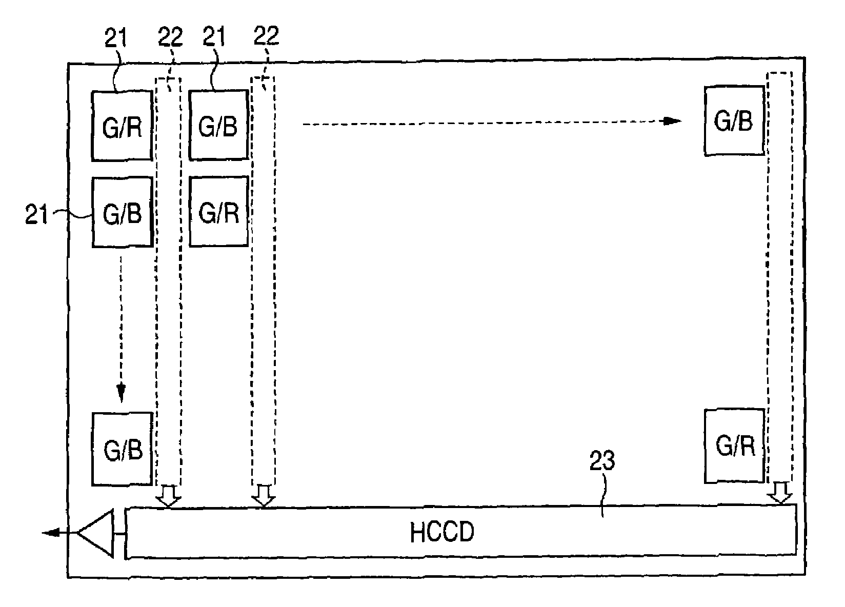
[0082]FIG. 10 is a schematic surface view of a CCD color solid-state image pickup device according to a second embodiment of the invention. In the drawing, a light-receiving section 21 is represented by a rectangle and taken as a unit pixel. A plurality of light-receiving sections 21 are arranged in an array pattern. In this embodiment, the light-receiving sections 21 are arranged in a square grid pattern. A vertical transfer path 22 is formed between horizontally-adjacent light-receiving sections 21. Signal charges read from the light-receiving section 21 to the vertical transfer path 22 are transferred to a horizontal transfer path 23 provided at a downward location. In the drawing, G / R and G / B are entered in each light-receiving section 21. However, these descriptions show that each unit pixel can subject R, G wavelength components and B, G wavelength components of the incident light to photoelectric conversion performed in the light-receiving section; the descriptions do not ind...

third embodiment

[0101]FIG. 16 is a schematic surface view of a CCD color solid-state image pickup device according to a third embodiment of the invention. The basic configuration of the present embodiment is analogous to that of the first embodiment. In contrast with the first embodiment in which the light-receiving section 10 detects signal electric charges of three colors; that is, R, G and B, the present embodiment differs in that a light-receiving section 40 of the present embodiment detects signal electric charges of two colors; that is, G and B and that a vertical-transfer path 41 per se is utilized as an R light receiving region. Here, the concept for utilizing the vertical transfer path 41 as a region for receiving light of a long wavelength (R) has already been known as described in, e.g., Japanese Patent No. 2534105.

[0102]In the embodiment, the vertical transfer path 41 is used as a light-receiving region for receiving light of a long wavelength (R). The original light-receiving section 4...


PUM


Abstract

A CCD color solid-state image pickup device has a plurality of light-receiving sections arranged in an array on the surface of a semiconductor substrate, and a vertical transfer path by way of which signal electric charges stored in electric charge storage sections of the respective light-receiving sections are read and transferred to a horizontal transfer path. In the image pickup device, the electric charge-storage section of each of the light-receiving sections has a plurality of electric charge storage layers which are provided in a depthwise direction of the semiconductor substrate with potential barriers interposed therebetween. Signal electric charges stored in the respective electric charge storage layers are read independently to the vertical transfer path.

Description

[0001]This Nonprovisional application claims priority under 35 U.S.C. § 119(a) on Patent Application No(s). 2003-065616 filed in JAPAN on Mar. 11, 2003, the entire contents of which is hereby incorporated by reference.BACKGROUND OF THE INVENTION[0002]1. Field of the Invention[0003]The present invention relates to a CCD (charge-coupled device) color solid-state image pickup device.[0004]2. Description of the Related Art[0005]In relation to a CCD semiconductor solid-state image pickup element and a CMOS semiconductor solid-state image pickup element, color filters having different spectral transmission coefficients are stacked on a plurality of photodiodes arranged in a two-dimensional array, thereby enabling pickup of a color image.[0006]In the color filters [red (R), green (G), and blue (B)] of primary color system, for instance, a B filter primarily permits passage of only light having a short wavelength of 470 nm or less. Hence, a photodiode of a light-receiving section with the B...

Claims


Application Information

Patent Timeline
Patent Type & Authority Patents(United States)
IPC IPC(8): H04N5/335H01L27/148H04N25/00
CPCH04N5/335H04N9/045H01L27/14868H01L27/14818H04N25/00
Inventor SHIZUKUISHI, MAKOTO
Owner FUJIFILM CORP
Features
  • R&D
  • Intellectual Property
  • Life Sciences
  • Materials
  • Tech Scout
  • Unparalleled Data Quality
  • Higher Quality Content
  • 60% Fewer Hallucinations
Learn More