Method of producing group 3 nitride substrate wafers and group 3 nitride substrate wafers

a technology of nitride substrate and nitride, which is applied in the direction of manufacturing tools, semiconductor/solid-state device details, lapping machines, etc., can solve the problems of more fragile wafers, more difficulty in planar processing, and difficult grinding, lapping and polishing of hard gan wafers, etc., to achieve low dislocation density, reduce dislocation density, and high concentration

Inactive Publication Date: 2010-02-16
SUMITOMO ELECTRIC IND LTD
View PDF9 Cites 3 Cited by
  • Summary
  • Abstract
  • Description
  • Claims
  • Application Information

AI Technical Summary

Benefits of technology

[0059]Grinding, lapping and polishing are three different processes for wafer surface planar-processing. Hitherto sometimes the word “polishing” is used as a collective concept for representing three different processes. Grinding is a step of roughly rubbing wafer surfaces with gross fixed whetting granules. Grinding eliminates large ruggedness, produces a flatter wafer surface and reduces a wafer thickness into a predetermined scope of thickness. Grinding is fastest in the speed of reducing a wafer thickness.
[0074]The present invention enables the surface planar wafers to make epitaxial layers endowed with excellent crystallography and morphology and to make devices excellent in quality and yield.

Problems solved by technology

Grinding, lapping and polishing of harder GaN wafers are more difficult than the planar-processing of Si wafers.
GaN wafers are more fragile than Si wafers, which makes more difficulty with the planar-processing of GaN wafers.
Small GaN crystals are useless for making devices.

Method used


Image

  • Method of producing group 3 nitride substrate wafers and group 3 nitride substrate wafers
  • Method of producing group 3 nitride substrate wafers and group 3 nitride substrate wafers
  • Method of producing group 3 nitride substrate wafers and group 3 nitride substrate wafers

Examples


embodiment 1

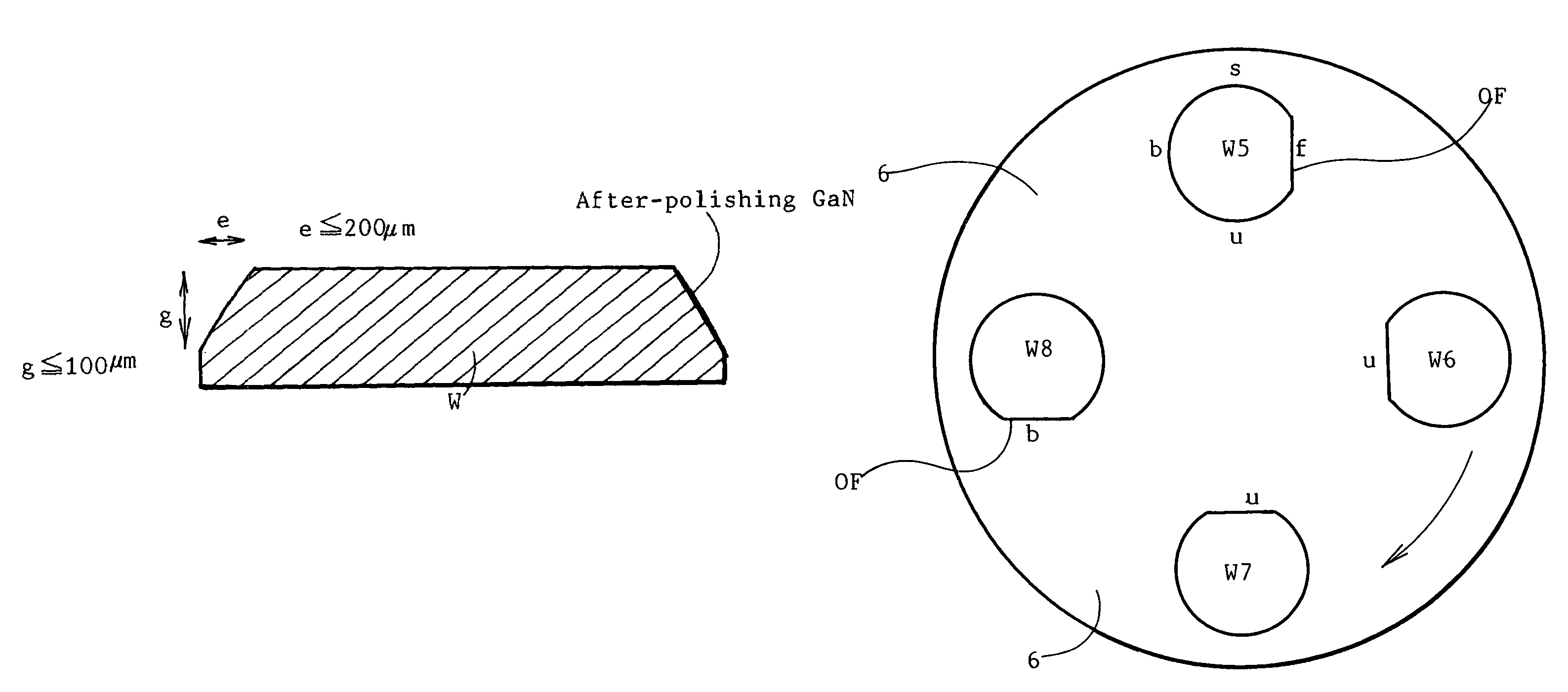
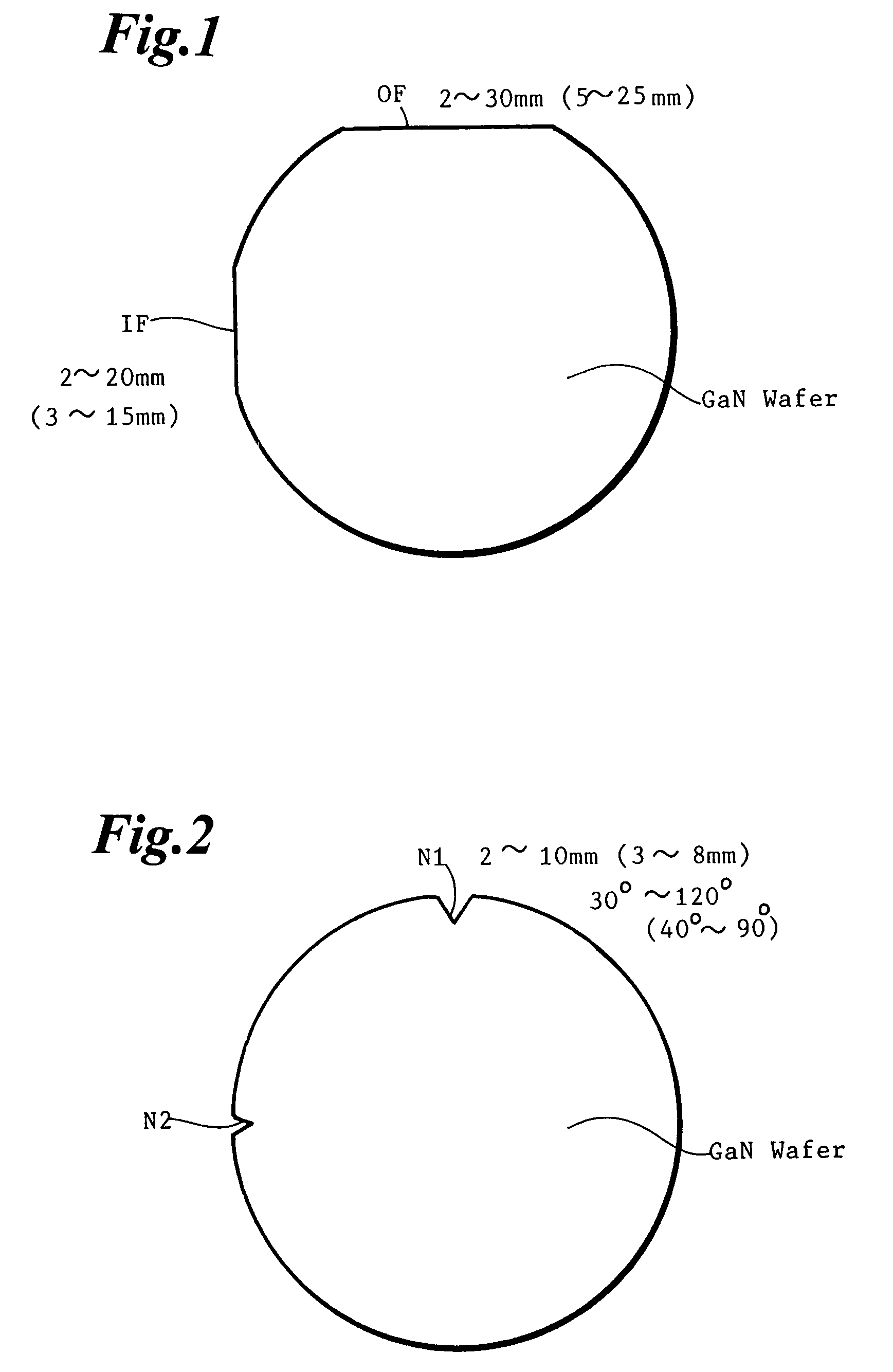
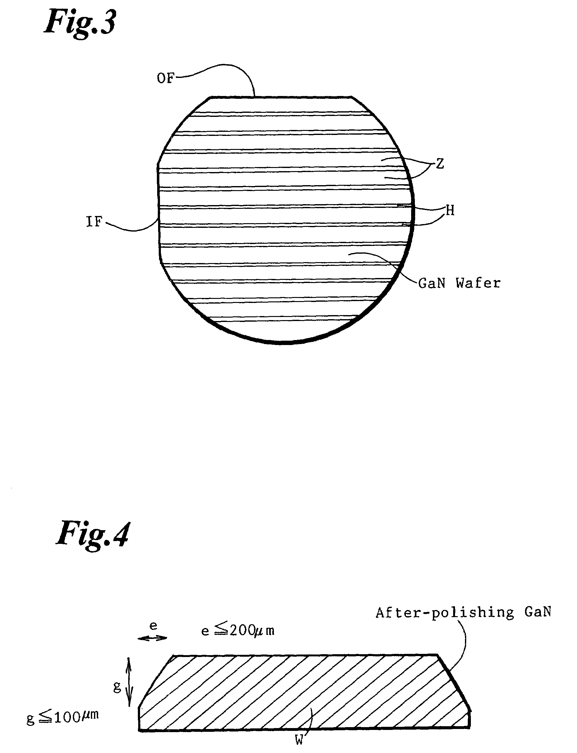
[0083]A polishing plate of an alumina (Al2O3) disc with a 135 mm diameter and a 30 mm thickness is prepared. Sample wafers of grinding, lapping and polishing are HVPE as-grown GaN circular wafers with a 50 mm diameter and a 0.5 mm thickness. An as-grown GaN ingot is obtained by growing a GaN crystal on a GaAs undersubstrate and eliminating the GaAs undersubstrate. A plurality of as-grown GaN substrate wafers are produced by slicing the GaN ingot by a wire-saw. Each as-grown wafer has an orientation flat (OF) of a 16 mm length. The central angle (τ) of OF is 18 degrees. The eliminated width h for OF is 0.6 mm. Each sample is a set of three as-grown wafers with an OF.

[0084]Three as-grown GaN wafers are pasted on the bottom of a polishing plate by heating the polishing plate up to a temperature of Tm+30° C., rubbing the bottom of the polishing plate with a thermoplastic solid wax, softening the wax, placing as-grown wafers at spots with a 5 mm margin p (p=5 mm) from the plate edge and ...

embodiment 2

[0108]Embodiment 2 employs a polishing plate of an alumina (Al2O3) disc with a 155 mm diameter and a 30 mm thickness. Object GaN wafers of grinding, lapping and polishing processes are sets of stripe structure HVPE-as-grown GaN wafers with a 50 mm diameter and a 0.5 mm thickness. The stripe structure means a non-uniform GaN crystal having reciprocally alternating sets of parallel low density single crystal regions and parallel defect accumulating regions. The stripe structure GaN wafers have been made by preparing a GaAs undersubstrate, producing a stripe mask on the GaAs undersubstrate, growing a GaN film crystal on the stripe-masked undersubstrate by an HVPE method, producing facets and maintaining the facet till the end. HVPE-as-grown GaN / GaAs complex wafers are made. An as-grown GaN freestanding wafer is obtained by removing the GaAs undersubstrate and chamfering an edge. Otherwise if a tall GaN crystal is grown on a GaAs undersubstrate for a long time by the HVPE method, a plur...


PUM

PropertyMeasurementUnit
lengthaaaaaaaaaa
diameteraaaaaaaaaa
thicknessaaaaaaaaaa

Abstract

Quality of one-surface planar processed group 3 nitride wafers depends upon a direction of pasting of wafers on a polishing plate. Low surface roughness and high yield are obtained by pasting a plurality of group 3 nitride as-grown wafers on a polishing plate with OFs or notches facing forward (f), backward (b) or inward (u) with thermoplastic wax having a thickness of 10 μm or less, grinding the as-grown wafers, lapping the ground wafers, polishing the lapped wafers into mirror wafers with a bevel of a horizontal width of 200 μm or less and a vertical depth of 100 μm or less.

Description

RELATED APPLICATIONS[0001]This application claims priority to Japanese Patent Application No. 2006-191000 filed Jul. 12, 2006 and Japanese Patent Application No. 2006-337678 filed Dec. 15, 2006.BRIEF DESCRIPTION OF THE INVENTION[0002]This invention relates to a method of sticking as-grown GaN, AlN or AlGaN substrate wafers to a polishing plate and grinding, lapping, and polishing the as-grown wafers into mirror wafers. GaN, AlN and AlGaN wafers are now collectively called “group 3 nitride” wafers. All the group 3 nitride crystals cannot be grown from liquid phase. As-grown substrate crystals of the group 3 nitrides are produced by growing a thick film on an undersubstrate in vapor phase, eliminating the undersubstrate and obtaining a freestanding wafer.[0003]Silicon (Si) substrate wafers are rich in toughness. Grinding, lapping and polishing are easy for silicon wafers. GaN is more rigid than Si, but is more fragile than Si. GaN is subject to external shock far more than Si. GaN is ...

Claims


Application Information

Patent Timeline
Patent Type & Authority Patents(United States)
IPC IPC(8): H01L21/304H01L29/30B24B37/30C04B41/91
CPCB24B37/042H01L21/02013H01L21/02027H01L21/6835H01L23/544H01L29/0657H01L2221/6834H01L2223/54493H01L2924/0002H01L2924/00H01L21/304H01L21/20
Inventor ISHIBASHI, KEIJIIRIKURA, MASATONAKAHATA, SEIJI
Owner SUMITOMO ELECTRIC IND LTD
Why Eureka
Try Eureka