Radiation-emitting and/or radiation-receiving semiconductor component and method for the production thereof

a technology of radiation-emitting and/or radiation-receiving semiconductors, applied in semiconductor devices, semiconductor/solid-state device details, electrical devices, etc., can solve the problem of comparatively high production expenditure of led package types, and achieve the effect of being easy to manufacture and sufficiently resistant to ageing

Active Publication Date: 2010-02-23
OSRAM OLED
View PDF35 Cites 27 Cited by
  • Summary
  • Abstract
  • Description
  • Claims
  • Application Information

AI Technical Summary

Benefits of technology

[0006]The object of the present invention is to improve a semiconductor component of the type cited at the beginning hereof in such fashion that it ...

Problems solved by technology

Due to the comparatively large number of package components, this...

Method used


Image

  • Radiation-emitting and/or radiation-receiving semiconductor component and method for the production thereof
  • Radiation-emitting and/or radiation-receiving semiconductor component and method for the production thereof
  • Radiation-emitting and/or radiation-receiving semiconductor component and method for the production thereof

Examples


Embodiment Construction

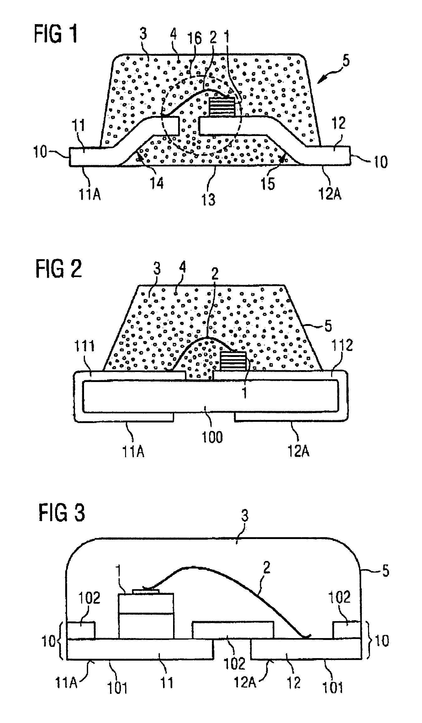
[0028]The first exemplary embodiment, illustrated in FIG. 1, is in the form of a leadframe-based, white-light-emitting light-emitting diode component.

[0029]A metallic leadframe 10, on which an LED chip 1 is mounted in a chip mounting region 16, is overmolded with a transparent silicone molding compound 3, from which a leadframe lead 11, 12 protrudes at each of two opposite lateral faces. Leadframe leads 11, 12 constitute the external electrical leads of the LED component. Inside the transparent silicone molding compound 3, each leadframe lead 11, 12 is provided with an S-shaped bend 14, 15 from a chip mounting region 16 to a mounting side 13 of the LED component.

[0030]To increase the refractive index, the silicone molding compound 3 can be admixed with at least one inorganic filler such as TiO2, ZrO2 or α-Al2O3.

[0031]In the method of making an LED light source according to FIG. 1, LED chip 1 is mounted on leadframe 10 in chip mounting region 16 and is connected electrically conducti...


PUM


Abstract

A radiation-emitting and/or radiation-receiving semiconductor component comprising a radiation-emitting and/or radiation-receiving semiconductor chip, a molded plastic part which is transparent to an electromagnetic radiation to be emitted and/or received by the semiconductor component and by which the semiconductor chip is at least partially overmolded, and external electrical leads that are electrically connected to electrical contact areas of the semiconductor chip. The molded plastic part is made of a reaction-curing silicone molding compound. A method of making such a semiconductor component is also specified.

Description

CROSS-REFERENCE TO RELATED APPLICATIONS[0001]This application is the National Stage of International Application No. PCT / DE2004 / 002738, filed on Dec. 14, 2004, which claims the priority to German Patent Applications Ser. No. 103 61801.5, filed on Dec. 30, 2003, and Ser. No. 20 2004005228.8, filed on Apr. 2, 2004. The contents of the prior applications are hereby incorporated by reference in their entireties.FIELD OF THE INVENTION[0002]The invention relates to a radiation-emitting and / or radiation-receiving semiconductor component comprising a radiation-emitting and / or radiation-receiving semiconductor chip, a molded plastic part which is transparent to an electromagnetic radiation to be emitted and / or received by the semiconductor component and by which the semiconductor chip is at least partially overmolded, and external electrical leads that are electrically connected to electrical contact areas of the semiconductor chip.BACKGROUND OF THE INVENTION[0003]Such semiconductor componen...

Claims


Application Information

Patent Timeline
IPC IPC(8): H01L23/31H01L31/0203H01L31/18H01L33/48H01L33/50H01L33/56H01L33/62
CPCH01L31/0203H01L33/56H01L33/62H01L33/486H01L2224/48091H01L33/501H01L2224/48228H01L2224/48247H01L2224/48472H01L2924/01004H01L2924/01078H01L2924/01068H01L2224/48227H01L2224/73265H01L2924/12041H01L2924/00H01L2924/00014
Inventor BRUNNER, HERBERTJAGER, HARALDSORG, JORG ERICH
Owner OSRAM OLED
Why Eureka
Try Eureka