Semiconductor device and manufacturing method thereof

a technology of semiconductor devices and manufacturing methods, applied in the direction of semiconductor devices, basic electric elements, electrical appliances, etc., can solve the problems of difficult implanting of impurities (e.g., boron) into the silicon layer, the requirement to suppress the diffusion of impurities in the silicon layer becomes harder, and the resistance cannot be reduced.

Active Publication Date: 2010-03-09
MICRON TECH INC
View PDF4 Cites 21 Cited by
  • Summary
  • Abstract
  • Description
  • Claims
  • Application Information

AI Technical Summary

Benefits of technology

[0010]Therefore, an object of the present invention is to provide a semiconductor device in which impurity can be sufficiently supplied into a silicon layer while suppressing diffusion of the impurity into a silicide layer without increase in resistance of a gate electrode, and to provide a method of manufacturing the semiconductor device.
[0015]As described above, according to the present invention, a semiconductor device is provided in which the diffusion of impurity into a silicide layer can be suppressed without increasing a resistance of a gate electrode, while sufficiently supplying the impurity in a silicon layer, and a manufacturing method of the semiconductor device is also provided.

Problems solved by technology

Thus, when the thickness of the laminate film is thick, reduction of the resistance cannot be attained.
However, a requirement to suppress the diffusion of impurity in the silicon layer becomes harder according to the thinning of the silicon layer for reducing the size of a semiconductor device.
When a silicon layer is thinned, it is hard to implant impurity (e.g., boron) into the silicon layer.
However, when the acceleration energy of the impurity reduces, an impurity concentration increases in the surface of the silicon layer.
Therefore, the impurity is not sufficiently supplied up to a portion of the silicon layer near the gate oxide film.
As a result, the operation characteristics of the semiconductor device are degraded due to a depletion layer.
Thus, it was made clear that the degradation in the operation characteristics of the semiconductor device accompanied by thinning of the silicon layer could not be completely suppressed even if the above-described conventional techniques were used.

Method used


Image

  • Semiconductor device and manufacturing method thereof
  • Semiconductor device and manufacturing method thereof
  • Semiconductor device and manufacturing method thereof

Examples


Embodiment Construction

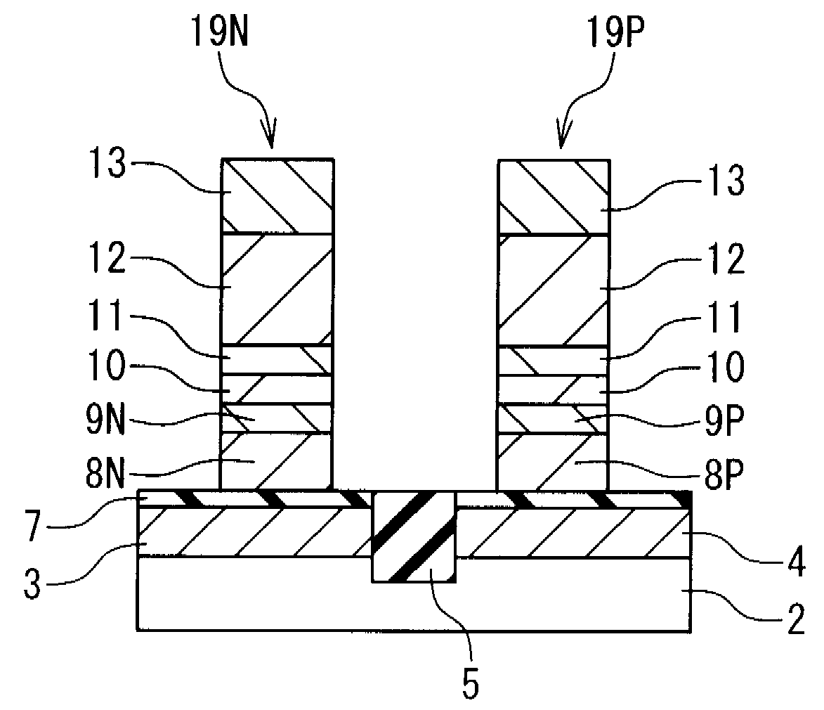
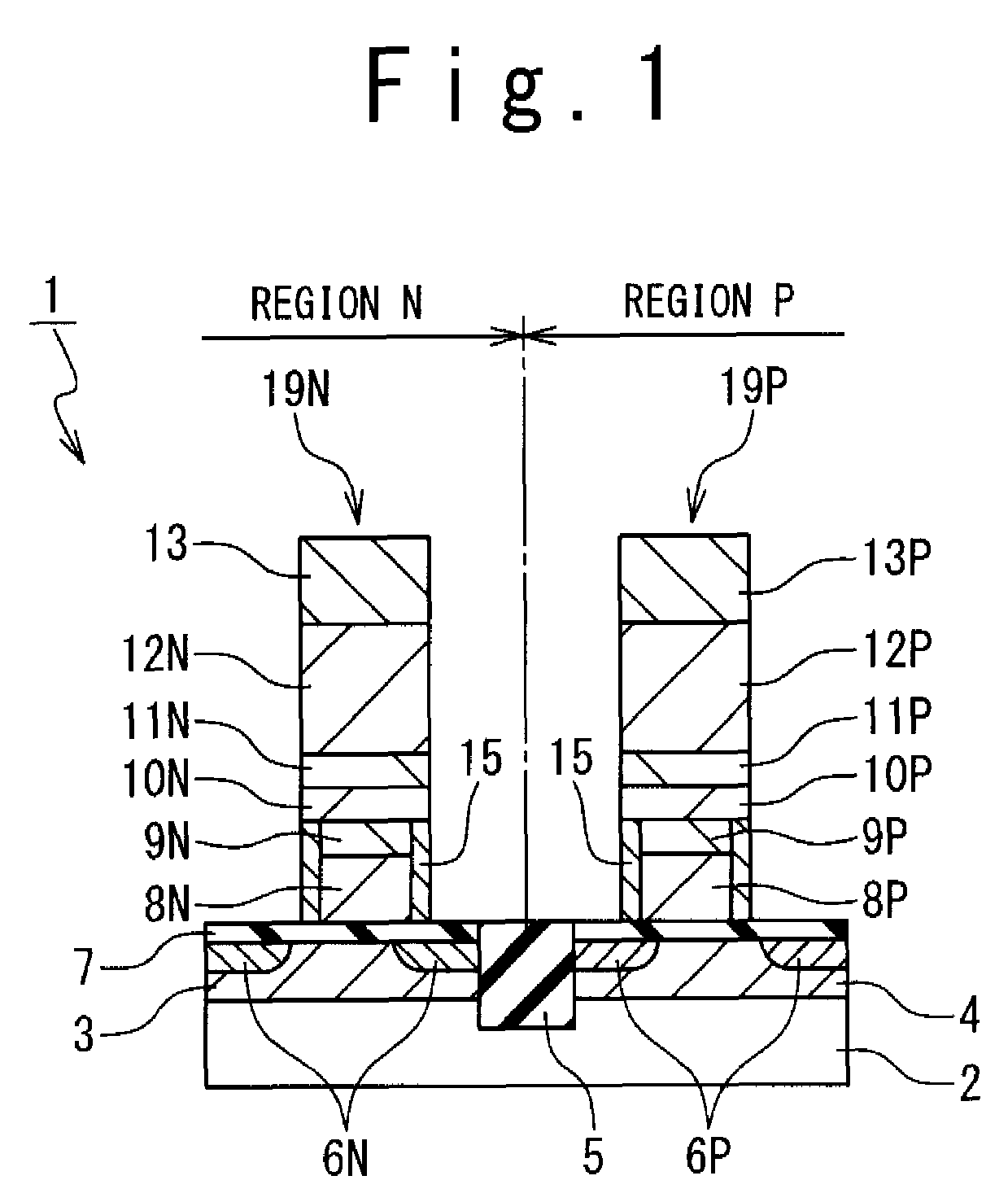
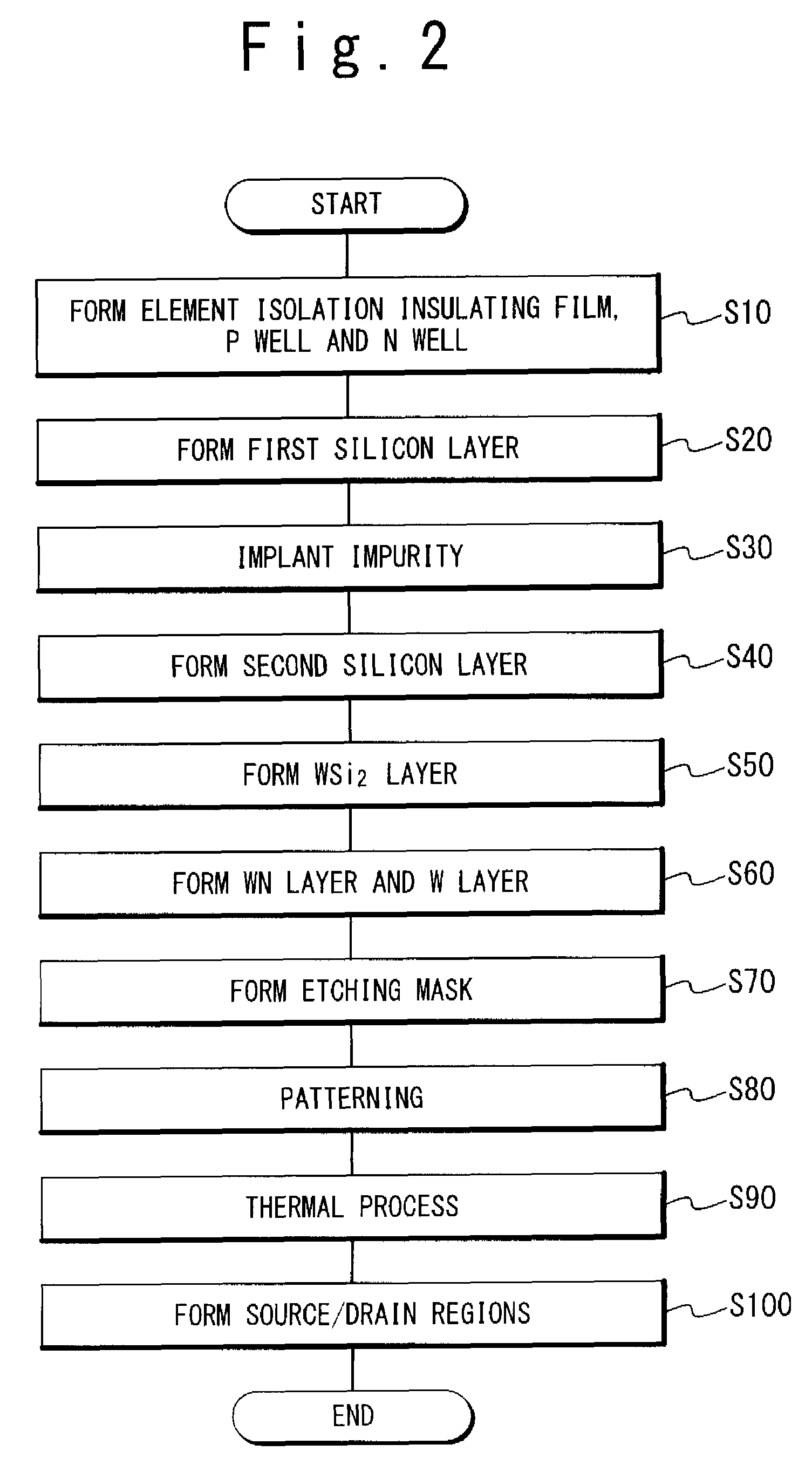
[0020]Hereinafter, a semiconductor device according to an embodiment of the present invention will be described in detail with reference to the attached drawings. FIG. 1 is a schematic cross sectional view showing a cross section structure of a semiconductor device 1 according to an embodiment of the present invention. As shown in FIG. 1, the semiconductor device 1 has a transistor structure formed on a semiconductor substrate 2. In this embodiment, the semiconductor device 1 has a dual gate structure in which an N channel transistor and a P-channel transistor are provided on the semiconductor substrate 2.

[0021]As shown in FIG. 1, an element isolation insulating film 5 is embedded in a surface of the semiconductor substrate 2. The element isolation insulating film 5 divides a semiconductor region into an N channel transistor formation region (to be described as a region N below) and a P-channel transistor formation region (to be described as a region P below). A gate insulating film...


PUM

PropertyMeasurementUnit
thicknessaaaaaaaaaa
thicknessaaaaaaaaaa
thicknessaaaaaaaaaa

Abstract

A semiconductor device includes an N-channel transistor having an N-type gate electrode and a P-channel transistor having a P-type gate electrode which are formed on a semiconductor substrate. The P-type gate electrode includes a first silicon layer formed as the lowest layer, and doped with a P-type impurity; a second silicon layer formed on the first silicon layer; and a metal containing layer formed on the second silicon layer. The N-type gate electrode includes a third silicon layer formed as the lowest layer and doped with an N-type impurity; a fourth silicon layer formed on the third silicon layer; and a metal containing layer formed on the fourth silicon layer. At least one of the second silicon layer and the fourth silicon layer is doped with no impurity or an impurity of a conductive type opposite to that of the impurity in a corresponding one of the first silicon layer and third silicon layer.

Description

BACKGROUND OF THE INVENTION[0001]1. Field of the Invention[0002]The present invention relates to a semiconductor device and a manufacturing method thereof. This application is based on Japanese Patent Applications 2006-347874 and 2007-281918. These disclosures of the above Japanese Patent Applications are incorporated herein by reference.[0003]2. Description of Related Art[0004]Recently, in a semiconductor device, particularly DRAM (Dynamic Random Access Memory), a polymetal gate structure is employed to improve a device operation speed. In the polymetal gate structure, a metal layer is formed on a polysilicon layer, so that this structure can further reduce a word line (sheet) resistance more than a polycide gate structure which was conventionally used. However, when the metal layer (e.g., a tungsten (W) layer) is formed directly on the polysilicon layer, the metal layer reacts with the polysilicon layer in a high temperature thermal treatment to form a metal silicide layer (e.g., ...

Claims


Application Information

Patent Timeline
Patent Type & Authority Patents(United States)
IPC IPC(8): H01L29/78
CPCH01L27/10891H01L21/28061H01L21/82345H10B12/488
Inventor TAGUWA, TETSUYA
Owner MICRON TECH INC
Why Eureka
Try Eureka