

Apparatus for the removal of a fluorinated polymer from a substrate and methods therefor
a fluorinated polymer and apparatus technology, applied in the direction of semiconductor/solid-state device testing/measurement, photosensitive materials, instruments, etc., can solve the problems of affecting device yield, affecting device yield, and weakening of organic bonds that are normally strong and adhesives will eventually peel or flake off,
- Summary
- Abstract
- Description
- Claims
- Application Information
AI Technical Summary
Benefits of technology
Problems solved by technology
Method used
Image

Examples
Embodiment Construction
[0029]The present invention will now be described in detail with reference to a few preferred embodiments thereof as illustrated in the accompanying drawings. In the following description, numerous specific details are set forth in order to provide a thorough understanding of the present invention. It will be apparent, however, to one skilled in the art, that the present invention may be practiced without some or all of these specific details. In other instances, well known process steps and / or structures have not been described in detail in order to not unnecessarily obscure the present invention.
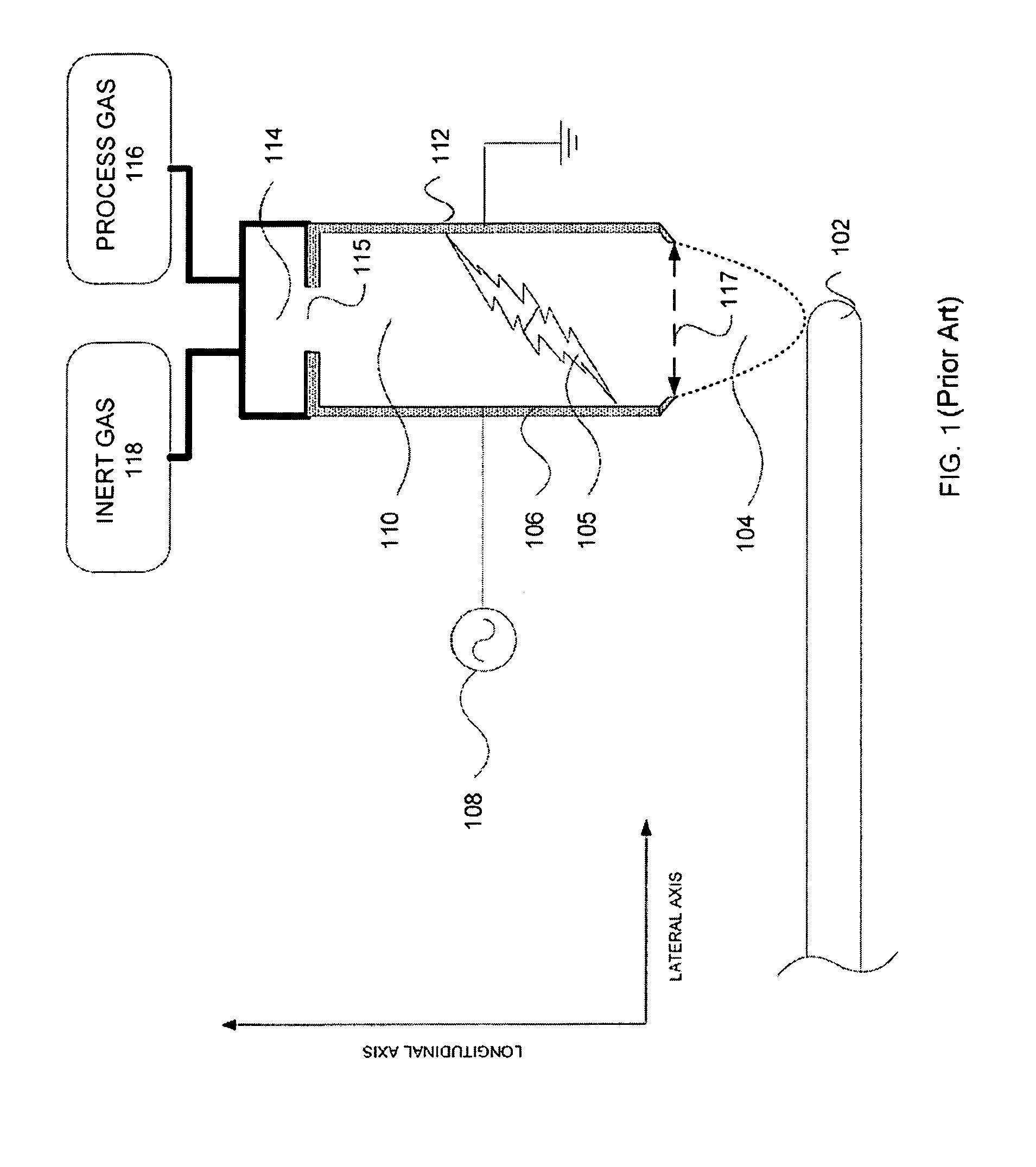
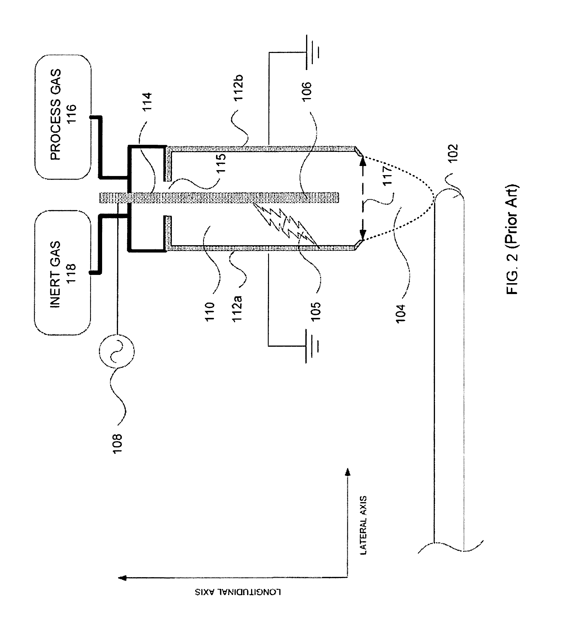
[0030]While not wishing to be bound by theory, the inventor believes that an atmospheric pressure plasma jet device, in which a dielectric barrier and a wire mesh are positioned between at least one electrode and a plasma (DWM-APPJ), may minimize arcing at a relatively low (less than 1 slm) inert gas flow rate, and hence may effectively remove a fluorinated polymer from a substrate.
[0031]I...
PUM
| Property | Measurement | Unit |
|---|---|---|
| pressure | aaaaa | aaaaa |
| surface area | aaaaa | aaaaa |
| diameter | aaaaa | aaaaa |
Abstract
Description
Claims
Application Information