
High dynamic range pre-power amplifier incorporating digital attenuator

a high-dynamic range, pre-power amplifier technology, applied in the field of data communication, can solve the problems of limited current consumption requirements for these transmit buffers, low power consumption of the transmit chain, and inability to maintain constant output power levels in amplitude-modulated, and achieve the effect of increasing the dynamic range of the switch array

Active Publication Date: 2010-04-06
TEXAS INSTR INC
View PDF7 Cites 13 Cited by
  • Summary
  • Abstract
  • Description
  • Claims
  • Application Information

AI Technical Summary

Benefits of technology

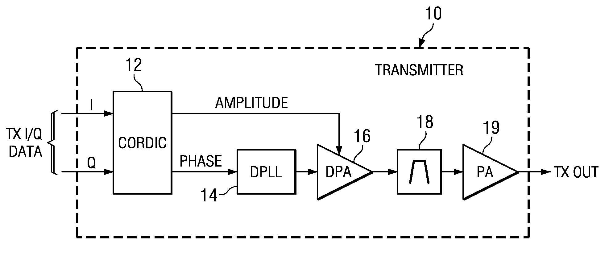
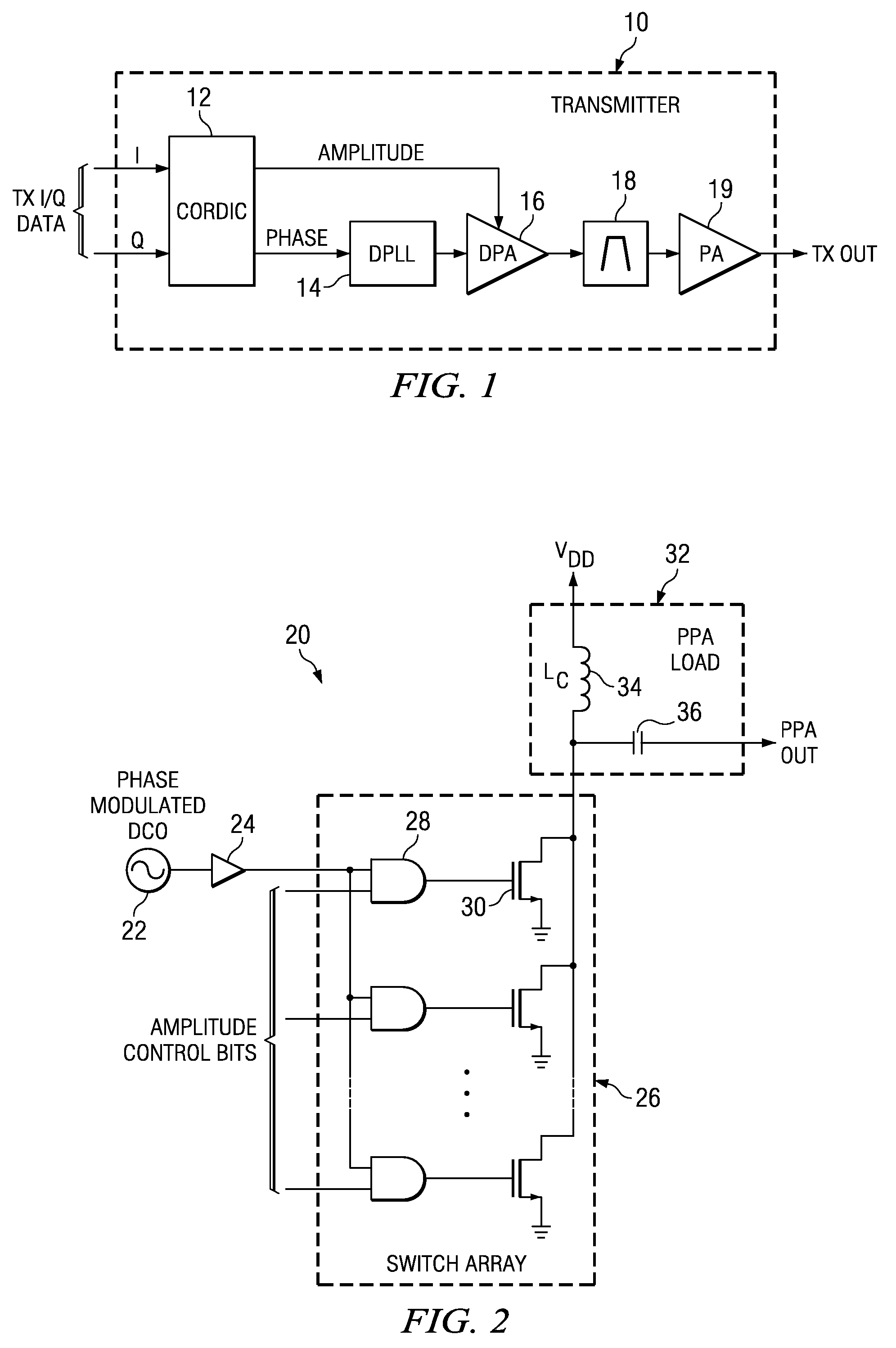
[0007]The present invention provides a solution to the problems of the prior art by providing a pre-power amplifier incorporating a digital attenuator circuit. The digital attenuator and associated pre-power amplifier are presented in the context of an all digital direct digital-to-RF amplitude converter (DRAC), which efficiently combines the traditional transmit chain functions of upconversion, I and Q combining, D / A conversion, filtering, buffering and RF output amplitude control into a single circuit.
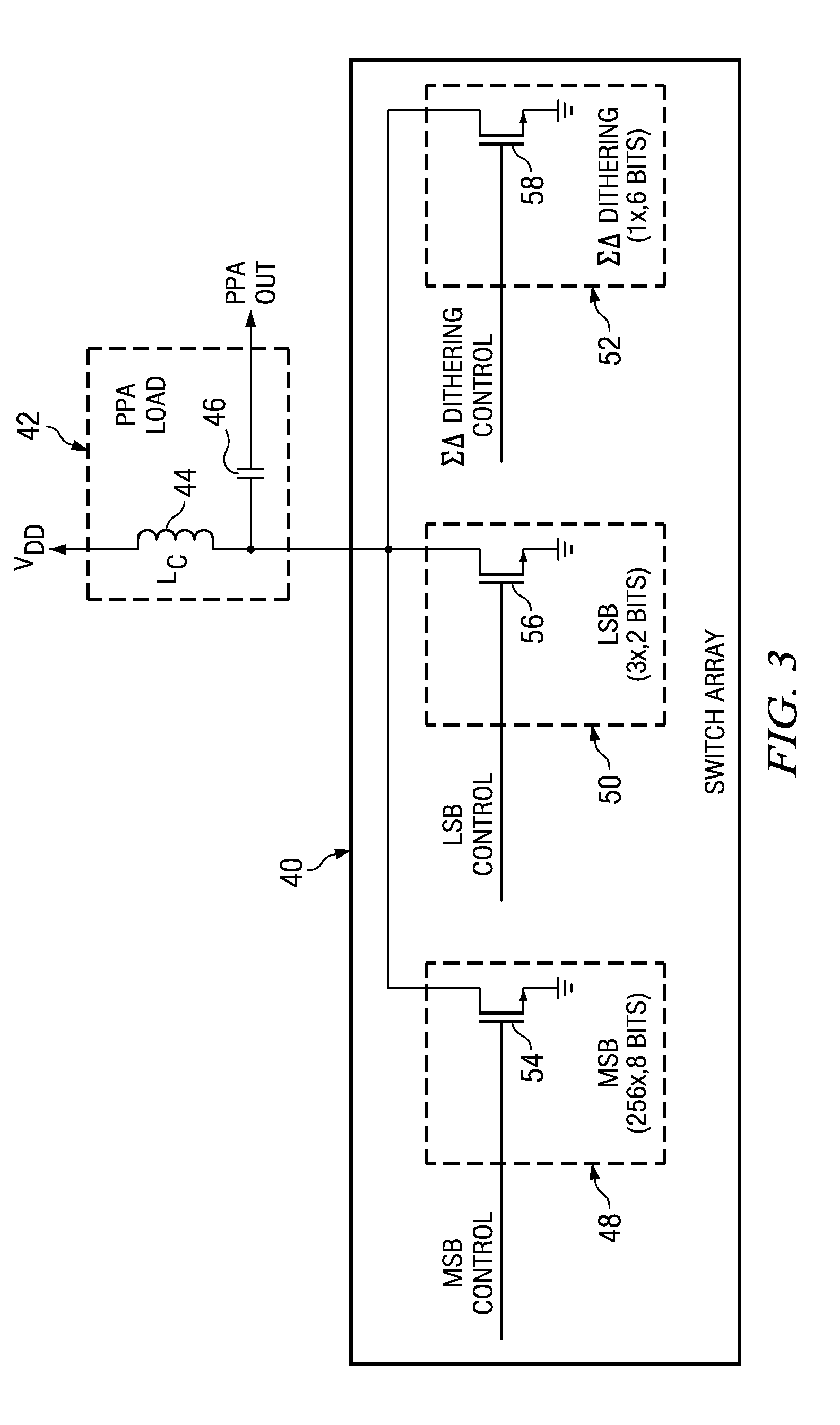
[0010]The digital attenuator is constructed as a segmented digitally controlled matrix or cell array comprising at least a pass and bypass matrix or array. Segmentation is dictated by the desire for small power control steps. The pass matrix controls the amount of current output from the PPA while the bypass matrix controls the amount of current shorted to the AC ground (i.e. power supply). By varying the number of transistors on or off in each matrix, the power output of the PPA can be easily and accurately controlled.
[0011]Several advantages of the attenuator include (1) guaranteed monotonicity, (2) power control is achieved without the need for a DAC, (3) minimum noise degradation, and (4) parasitic capacitance will not dominate the output assuming moderate attenuation of approximately 20 dB.
[0013]There is thus provided in accordance with the invention, a current attenuator for increasing the dynamic range of a signal generated by a circuit, comprising pass means for controlling the amount of current generated by the circuit that is passed through to the output of the circuit and bypass means for shorting a portion of current generated by the circuit to AC ground thereby reducing the signal output from the circuit.
[0015]There is further provided in accordance with the invention, a pre-power amplifier, comprising a load coupled to a power source, a switch array comprising a plurality of switches, the switch array for generating a current proportional to the number of switches active therein, an attenuator coupled to the load and the switch array comprising pass means for controlling the amount of current generated by the switch array that is passed through to the output of the pre-power amplifier and bypass means for shorting a portion of current generated by the switch array to AC ground thereby reducing signal to the output of the pre-power amplifier.
[0016]There is also provided in accordance with the invention, a pre-power amplifier, comprising a load coupled to a power source, a switch array comprising a plurality of switches, the switch array for generating a current proportional to the number of switches active therein and an attenuator for increasing the dynamic range of the switch array, the attenuator comprising a pass transistor cell array coupled in series to the load and the switch array and operative to control the amount of current generated by the switch array that is passed through to the output of the pre-power amplifier, a bypass transistor cell array coupled to the switch array and AC ground and operative to short a portion of current generated by the switch array to AC ground thereby reducing signal to the output of the pre-power amplifier.

Problems solved by technology

In addition, the current consumption requirements for these transmit buffers are limited such that any gain control scheme cannot ‘burn’ or waste current in order to meet the power consumption budget and the strict signal to noise requirements stated above.
This output power level, however, is not constant in amplitude-modulated standards, such as EDGE, and must be controlled with appropriate variable-gain circuitry.
In these architectures, the overall power consumption of the transmit chain, including all the DAC and variable gain buffer components, is at least 50 mW which is a relatively high amount of power.

Method used


Image

  • High dynamic range pre-power amplifier incorporating digital attenuator
  • High dynamic range pre-power amplifier incorporating digital attenuator
  • High dynamic range pre-power amplifier incorporating digital attenuator

Examples


Embodiment Construction

Notation Used Throughout

[0033]The following notation is used throughout this document.

[0034]

TermDefinitionACAlternating CurrentASICApplication Specific Integrated CircuitCDMACode Division Multiple AccessCMOSComplementary Metal Oxide SemiconductorCWContinuous WaveDACDigital to Analog ConverterDCDirect CurrentDCODigital Controlled OscillatorDEMDynamic Element MatchingDPADigital Power AmplifierDPLLDigital Phase Locked LoopDRACDigital to RF Amplitude ConverterDRPDigital RF Processor or Digital Radio ProcessorDSPDigital Signal ProcessorEDGEEnhanced Data rates for Global EvolutionFPGAField Programmable Gate ArrayGPRSGeneral Packet Radio ServiceGSMGlobal System for Mobile CommunicationICIntegrated CircuitLSBLeast Significant BitLUTLook Up TableMSBMost Significant BitNFETn-channell Field Effect TransistorNMOSn-channel Metal Oxide SemiconductorPAPower AmplifierPMOSp-channel Metal Oxide SemiconductorPPAPre-Power AmplifierPVTProcess Voltage TemperatureRFRadio FrequencySAWSurface Acoustic WaveS...


PUM


Abstract

A novel digital attenuator circuit and associated pre-power amplifier (PPA) that substantially increases the dynamic range of the amplifier. Increased dynamic range is achieved by placing a digital current attenuator circuit at the output of the pre-power amplifier so that the minimum possible current output of the transistor switch array of the PPA can be further attenuated. The attenuator functions to split the current between the load and the power supply VDD (i.e. AC ground) based on device ratio that is controlled digitally via an input power control word. The digital attenuator is constructed as a segmented digitally controlled matrix or cell array comprising at least a pass and bypass matrix or array. The pass matrix controls the amount of current output from the PPA while the bypass matrix controls the amount of current shorted to the AC ground (i.e. power supply). By varying the number of transistors on or off in each matrix, the power output of the PPA can be easily and accurately controlled.

Description

FIELD OF THE INVENTION[0001]The present invention relates to the field of data communications and more particularly relates to a high dynamic range pre-power amplifier incorporating a digital attenuator for use in the transmitter portion of a Digital RF Processor or Digital Radio Processor (DRP).BACKGROUND OF THE INVENTION[0002]It is well known in the communication arts that a transmit (Tx) buffer is required for both wired and wireless communications systems to interface the transmit path signal to the outside environment. In many cases, the transmit buffer is required to apply a variable gain to the transmit signal in order to increase or reduce the amplitude of the output signal. One such case occurs when the transmitted signal is part of an amplitude modulated communication system and the transmit buffer itself is used to implement the amplitude modulation function. The signal to noise ratio (SNR) requirements of such Tx buffers in most systems are extremely strict, meaning that...

Claims


Application Information

Patent Timeline
Patent Type & Authority Patents(United States)
IPC IPC(8): H04B1/04H01Q11/12
CPCH03F1/0205H03F1/0277H03F3/211H03F3/72H04B1/0483H03G1/0088H03G3/001H03F2200/366H03F2203/21145H03F2200/331
Inventor LITMANEN, PETTERI M.LIN, HENG-CHIH
Owner TEXAS INSTR INC
Learn More