Thermal management substrate

a technology of thermal management substrate and substrate, which is applied in the direction of polycrystalline material growth, crystal growth process, gel state, etc., can solve the problems of insufficient thermal contact, lack of mechanical strength, and inability to withstand normal handling of linn patent, so as to improve the flatness and surface finish of the wafer

Inactive Publication Date: 2010-04-13
HRL LAB
View PDF25 Cites 24 Cited by
  • Summary
  • Abstract
  • Description
  • Claims
  • Application Information

AI Technical Summary

Benefits of technology

[0008]The present invention relates to fabricating a thermal management substrate. In one aspect, the method comprises acts of fabricating a separation by implantation of oxygen (SIMOX) wafer by ion-implantation; the SIMOX wafer including a Si wafer, a Si overlay structure, and a buried oxide (BOX) layer between the Si wafer and the Si overlay structure; depositing a polycry

Problems solved by technology

The efficiency with which heat is dissipated from digital ICs is currently limited by thermal conductance properties of the Si substrate.
However, the The Annamalai Patent, describes Si-on-diamond substrates being bonded to a carrier wafer, because they do not pos

Method used


Image

  • Thermal management substrate
  • Thermal management substrate
  • Thermal management substrate

Examples


Embodiment Construction

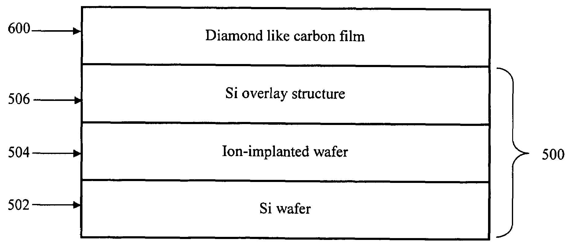
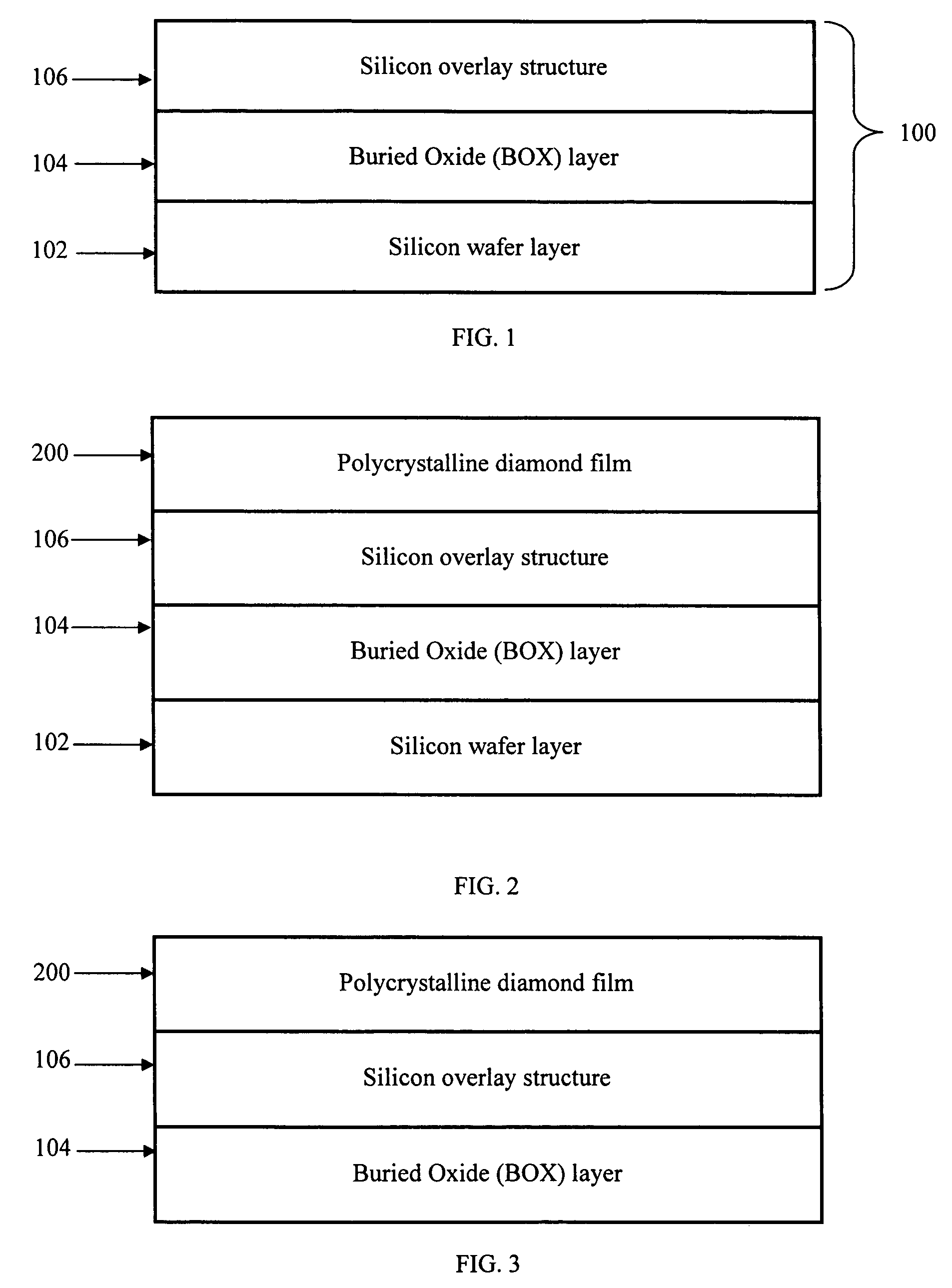
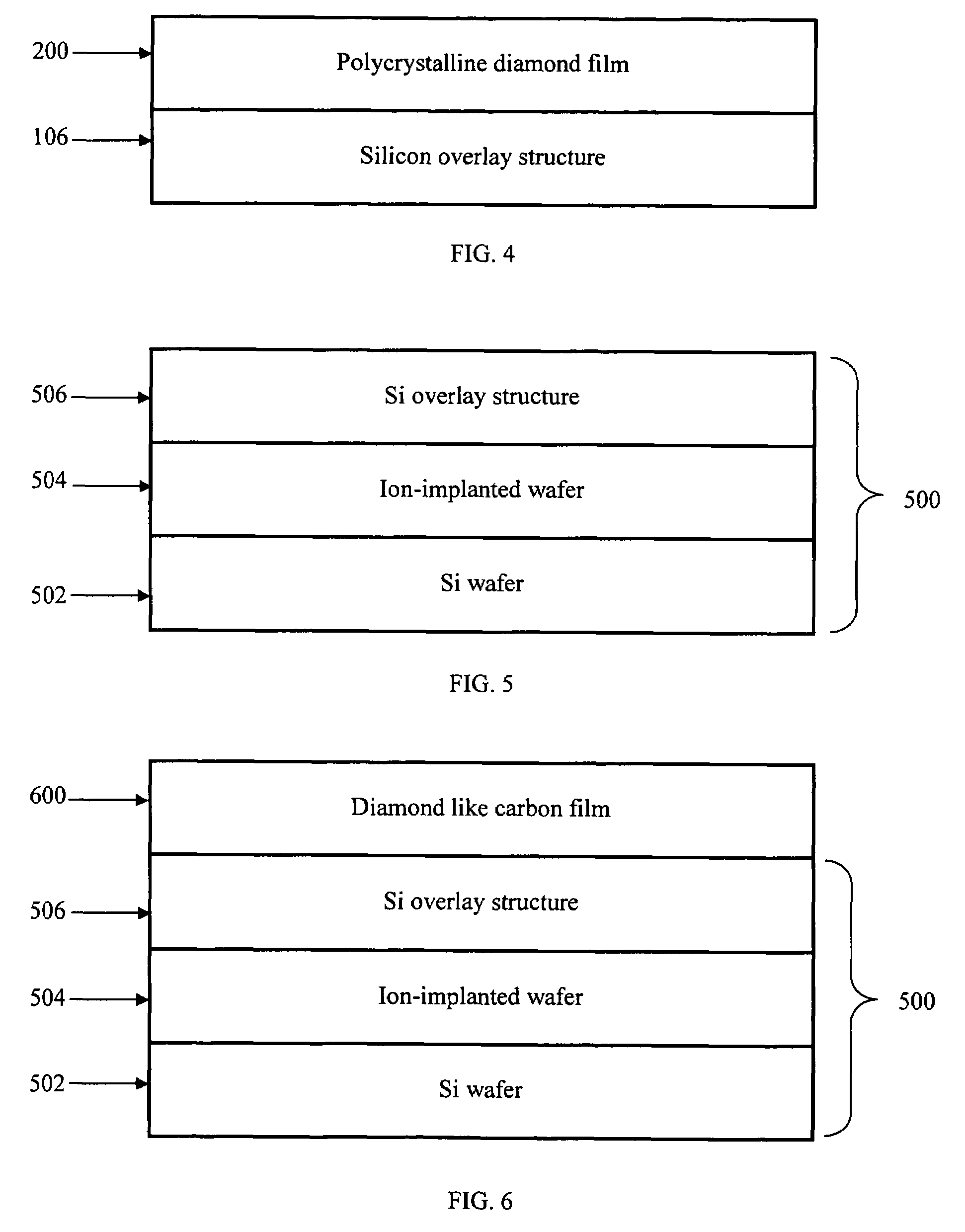
[0032]The present invention relates to a process used for fabricating Si-on-diamond or on diamond-like-carbon (DLC) wafers, and more particularly, Si-on-diamond or on DLC wafers that can be used as thermal management substrates. The following description is presented to enable one of ordinary skill in the art to make and use the invention and to incorporate it in the context of particular applications. Various modifications, as well as a variety of uses in different applications will be readily apparent to those skilled in the art, and the general principles defined herein may be applied to a wide range of embodiments. Thus, the present invention is not intended to be limited to the embodiments presented, but is to be accorded the widest scope consistent with the principles and novel features disclosed herein.

[0033]In the following detailed description, numerous specific details are set forth in order to provide a more thorough understanding of the present invention. However, it wil...


PUM


Abstract

The present invention is directed to a method for fabricating a thermal management substrate having a Silicon (Si) layer on a polycrystalline diamond film, or on a diamond-like-carbon (DLC) film. The method comprises acts of fabricating a separation by implantation of oxygen (SIMOX) wafer; depositing a polycrystalline diamond film onto the SIMOX wafer; and removing various layers of the SIMOX wafer to leave a Si overlay layer that is epitaxially fused with the polycrystalline diamond film. In the case of the DLC film, the method comprises acts of ion-implanting a Si wafer; depositing an amorphous DLC film onto the Si wafer; and removing various layers of the Si wafer to leave a Si overlay structure epitaxially fused with the DLC film.

Description

BACKGROUND OF THE INVENTION[0001](1) Field of Invention[0002]The present invention relates to a process used for fabricating Si-on-diamond or on diamond-like-carbon (DLC) wafers, and more particularly, Si-on-diamond or on DLC wafers that can be used as thermal management substrates.[0003](2) Description of Related Art[0004]Silicon (Si) wafers have long been used as substrates for fabricating circuits, such as Ultra Large Scale of Integration (ULSI) circuits. The Si wafers have typically been homogeneous Si monocrystalline wafers and separation by implantation of oxygen (SIMOX) wafers.[0005]High speed ULSI Complimentary Metal Oxide Semiconductor (CMOS) digital Integrated Circuits (ICs) generate more heat per unit chip area as levels of integration and clock rates are increased. Heat management is currently one of the major considerations in designs of ULSI digital ICs. Effective heat management will become increasingly more important as IC integration starts expanding into a third di...

Claims


Application Information

Patent Timeline
IPC IPC(8): C30B25/02
CPCH01L21/76254
Inventor MICOVIC, MIROSLAVDEELMAN, PETERROYTER, YAKOV
Owner HRL LAB
Why Eureka
Try Eureka