Semiconductor device with metal oxides and an organic compound

a technology of metal oxides and semiconductors, applied in thermoelectric devices, bulk negative resistance effect devices, instruments, etc., can solve the problems of difficult preventing crosstalk and needing to solve passive matrix elements, and achieve the effect of high integration and exceptionally low manufacturing costs per memory elemen

Inactive Publication Date: 2010-05-18
SEMICON ENERGY LAB CO LTD
View PDF23 Cites 69 Cited by
  • Summary
  • Abstract
  • Description
  • Claims
  • Application Information

AI Technical Summary

Benefits of technology

[0010]Because a passive matrix element has such a simple structure, a high level of integration of a memory cell in a passive matrix element becomes potentially possible.
[0022]By adoption of the structures described above, a selected memory cell can be addressed electrically without any crosstalk occurring even if passive matrix memory devices are used, and the resistance of the memory cell can be changed dramatically. Alternatively, the film thickness of the organic layer can be partially changed, and, as a result, the resistance of the memory cell can be greatly changed. By writing of data to the addressed memory cell, an electrical path including a layered structure of the lower electrode, the n-type metal oxide layer, the p-type metal oxide layer, and the upper electrode or an electrical path including a layered structure of the upper electrode, the n-type metal oxide layer, the p-type metal oxide layer, and the lower electrode is formed. In these layered structures, a p-n junction is formed between the p-type metal oxide layer and the n-type metal oxide layer, whereby a rectification characteristic can be obtained. As a result, malfunction of the memory device caused by the aforementioned crosstalk can be eliminated, and a memory device with a high level of integration can be obtained.
[0025]By use of the structure in FIG. 1C, the film thickness of the organic compound layer changes by writing of data to the memory cell, whereby a structure is provided in which the p-type metal oxide layer and the n-type metal oxide layer come into partial contact with each other to form a p-n junction. As a result, a rectification characteristic is manifested. Consequently, the crosstalk problem is eliminated, and a memory device with a high level of integration can be provided.
[0032]In addition, for prevention of falsification or misuse of data, when an organic material or inorganic material that does not undergo a reversible phase change is used as a material of the layer that contains an organic compound of the memory element, writing of data to an individual memory cell is set to be performed once.
[0034]By the present invention, a high-yield manufacturing process of a memory device is realized, and a semiconductor device using memory elements for which manufacturing costs per memory element are exceptionally low can be provided. In addition, a semiconductor device using memory devices with a high level of integration can be provided.

Problems solved by technology

However, there is a serious problem with passive matrix elements that needs to be solved.
However, there is a problem in that preventing crosstalk is technically difficult.

Method used


Image

  • Semiconductor device with metal oxides and an organic compound
  • Semiconductor device with metal oxides and an organic compound
  • Semiconductor device with metal oxides and an organic compound

Examples


embodiment mode 1

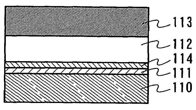
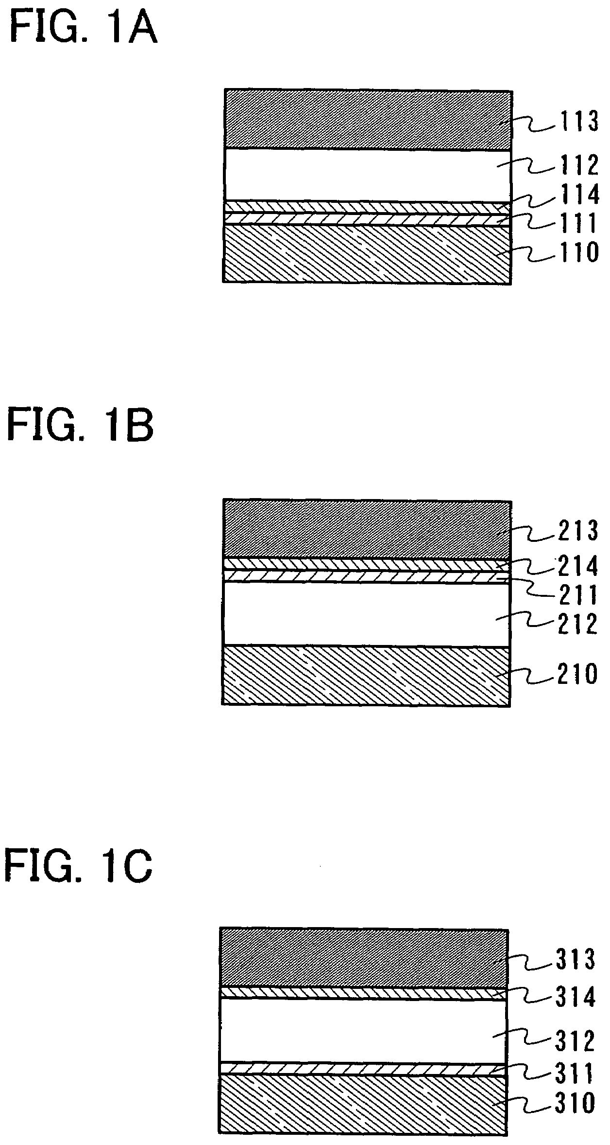
[0046]In the present embodiment mode, an example of a manufacturing method of a passive matrix memory device that has a plurality of memory elements over a glass substrate, which is one kind of a substrate that has an insulating surface, will be explained using FIG. 1A. FIG. 1A is a cross-sectional view schematic diagram of one memory element.

[0047]First, over a glass substrate, a first electrode 110 is formed as shown in FIG. 1A. The first electrode 110 can be formed as a single-layer or multilayer structure. Specifically, a film of elemental aluminum (Al), titanium (Ti), molybdenum (Mo), tungsten (W), a film of an alloy using one or more of any of these elements, a film of an alloy of one or more of any of these elements and silicon, or the like can be used. Alternatively, a light-transmitting material such as indium-tin oxide (ITO), indium-tin oxide containing silicon oxide, indium oxide containing from 2 wt % to 20 wt % of zinc oxide, or the like can also be used.

[0048]It is to ...

embodiment mode 2

[0054]In Embodiment Mode 1, an example is given of a memory element in which metal oxide layers are stacked to form a p-n junction and a layer containing an organic compound over the stacked layers. In the present embodiment mode, an example will be given of a memory element that has a first metal oxide layer and a second metal oxide layer stacked over a layer that contains an organic compound in such a way that a p-n junction is formed.

[0055]First, over a glass substrate, as in Embodiment Mode 1, a first electrode 210 is formed as shown in FIG. 1B.

[0056]Next, a partition is provided to separate neighboring memory elements, that is, neighboring first electrodes 210. In the present embodiment mode, the partition is provided; however, the partition need not necessarily be used.

[0057]Next, a layer 212 that contains an organic compound is formed over the first electrode 210. The layer 212 that contains an organic compound can be formed by an evaporation method, a spin coating method, a ...

embodiment mode 3

[0063]In the present embodiment mode, an example of a memory element is shown in which a layer that contains an organic compound is provided over a first metal oxide layer, and a second metal oxide layer is provided over the layer that contains an organic compound.

[0064]First, over a glass substrate, as in Embodiment Mode 1, a first electrode 310 is formed as shown in FIG. 1C.

[0065]Next, a partition is provided to separate neighboring memory elements, that is, neighboring first electrodes 310.

[0066]Next, a first metal oxide layer 311 that functions as a p-type semiconductor material is formed over the first electrode 310.

[0067]Then, a layer 312 that contains an organic compound is formed over the first metal oxide layer 311.

[0068]After that, a second metal oxide layer 314 that functions as an n-type semiconductor material is formed over the layer 312 that contains an organic compound.

[0069]In the present embodiment mode, because the layer 312 that contains an organic compound is for...


PUM

PropertyMeasurementUnit
thicknessaaaaaaaaaa
thicknessaaaaaaaaaa
thicknessaaaaaaaaaa

Abstract

A semiconductor memory device is disclosed in which a layer containing an organic compound is interposed between a pair of electrodes and, further, a first layer including a first metal oxide and a second layer including a second metal oxide are interposed between the pair of electrodes. One of the two layers including the metal oxide acts as a p-type semiconductor layer and the other acts as an n-type semiconductor layer. The first layer including the first metal oxide and the second layer including the second metal oxide form a p-n junction, which provides rectification characteristic to the semiconductor memory device.

Description

BACKGROUND OF THE INVENTION[0001]1. Field of the Invention[0002]The present invention relates to a semiconductor device which stores data.[0003]The present invention relates to a semiconductor device that includes a memory element and a circuit, which includes a thin film transistor (hereinafter referred to as a TFT), and a manufacturing method thereof.[0004]It is to be noted that a semiconductor device in the present specification corresponds to a semiconductor device that can function as a general device by use of semiconductor characteristics, and electro-optical devices, semiconductor circuits, and electronic devices can all be considered semiconductor devices.[0005]2. Description of the Related Art[0006]Individual identification technology using semiconductor devices in which data is exchanged by wireless communication has been attracting attention in recent years. Individual identification technology using semiconductor devices has started to be utilized in production, managem...

Claims


Application Information

Patent Timeline
Patent Type & Authority Patents(United States)
IPC IPC(8): H01L35/24
CPCH01L27/1021
Inventor NOMURA, RYOJITOKUNAGA, HAJIMEKATO, KIYOSHI
Owner SEMICON ENERGY LAB CO LTD
Why Eureka
Try Eureka