Nanowire structures and electrical devices

a wire structure and wire technology, applied in the field of nanotechnology, can solve the problems of low cooling, difficult fabrication of electronic devices and device components with dimensions below 10 nm, and washed out coulomb blockage via thermal fluctuations, and achieve good placement accuracy and reduce cross sectional dimensions

Inactive Publication Date: 2010-07-06
THE BOARD OF TRUSTEES OF THE UNIV OF ILLINOIS
View PDF5 Cites 9 Cited by
  • Summary
  • Abstract
  • Description
  • Claims
  • Application Information

AI Technical Summary

Benefits of technology

[0009]The present invention provides structures and devices comprising conductive segments and conductance constricting segments of a nanowire, such as metallic, superconducting or semiconducting nanowires. Particularly, structures of the present invention comprise conductive segments and conductance constricting segments having positions along the length of a nanowire selected with good placement accuracy. In addition, the present invention provides structures and devices comprising conductive nanowire segments and conductance constricting nanowire segments having accurately selected phases including crystalline and amorphous states, compositions, morphologies and physical dimensions, including selected cross sectional dimensions, shapes and lengths along the length of a nanowire. Further, the present invention provides methods of processing nanowires capable of patterning a nanowire to form a plurality of conductance constricting segments having selected positions along the length of a nanowire, including conductance constricting segments having reduced cross sectional dimensions and conductance constricting segments comprising one or more insulating materials such as metal oxides. Processing methods of the present invention are capable of providing local modification of the shape of selected regions of a nanowire with a resolution equal to about 3 nanometers.
[0012]First conductance constricting segments, second conductance constricting segments and / or the middle conductive segments of this aspect of the present invention may have electrical properties, such as conductances, electrical resistances and capacitances, selected for a given application, such as use in a nanoelectrical or nanoelectromechanical device. For example, in one useful embodiment the first conductance constricting segment, second conductance constricting segment or both have a resistance equal to or greater than about 12 kΩ, and preferably for some applications equal to or greater than about 25 kΩ. Alternatively, first conductance constricting segment, second conductance constricting segment or both may comprise thin insulating nanowire segments, such as metal oxide segments. High resistance and / or insulating conductance constricting segments are useful for limiting the propagation of electrons in a manner localizing the electronic wave functions of electrons in the middle conductive segment, for example to generate a middle conductive segment comprising a Coulomb island. In one embodiment, for example, the presence of first and second high resistance and / or insulating conduction constricting segments prevents mixing of the electronic states of electrons on the middle conductive segment with external states, thereby providing electron confinement in a Coloumb island of a SET transistor. The present invention also provides nanowire configurations having a middle conductive element with a capacitance low enough to provide a charging energy that is greater, for example a factor of 10 times greater, than thermal electronic fluctuations at a selected temperature, such a capacitance low enough to provide a charging energy that is less than thermal electronic fluctuations at room temperature (298K).
[0014]In an embodiment, conductance constricting segments of the present invention have average cross sectional dimensions equal to about 6 nanometers or less, and preferably for some applications equal to about 3 nanometers or less. In an embodiment, conductance constricting segments of the present invention extend along the length of the nanowire distances equal to a value selected over the range of about 1 nanometer to about 100 nanometers. Selection of the cross sectional dimension and length provides conductance constricting segments having an accurately selected electrical resistance, including high resistance conductance constricting segments. Selection of narrow cross sectional dimensions, for example cross sectional dimensions less than about 5 nanometers, allows fabrication of insulating conductance constricting segments via oxidation initiated by exposure of narrow conductance constricting segments to an oxidizing medium such as oxygen.
[0015]In an embodiment, the middle conductive segment has an average cross sectional dimension equal to or less than about 10 nanometers, more preferably for some applications equal to or less than about 6 nanometers. In an embodiment, the middle conductive segment extends along the length of the nanowire a distance equal to or less than about 20 nanometers, more preferably for some applications equal to or less than about 10 nanometers. Selection of small cross sectional dimensions, for example cross sectional dimensions less than about 6 nanometers, and short lengths, for example lengths less than about 10 nanometers, achieves capacitances and charging energies providing middle conductive segments useful as Coulomb islands in SET transistors.
[0017]In one embodiment, the positions of conductance constricting segments and conductive segments along the length of the nanowire are selected with great placement accuracy. For example, selection of the positions of first and second position of conductance constricting segments along the length of a nanowire to within about 10 nanometers or less provides a means of selecting the length of the middle conductive segment with good accuracy

Problems solved by technology

For example, a significant problem of SET transistors fabricated using photolithography methods and having a Coulomb island with physical dimensions equal to or greater than about 20 nanometers is that they must be cooled down to low temperatures to achieve useful device performance.
The fundamental problem with these devices is that the Coulomb blockage is washed out via thermal fluctuations if the energy that is necessary to add an electron to the Coulomb island is smaller than the characteristic thermal energy (kBT).
Fabrication of electronic devices and device components with dimensions below 10 nm, however, remains very challenging.

Method used


Image

  • Nanowire structures and electrical devices
  • Nanowire structures and electrical devices
  • Nanowire structures and electrical devices

Examples


example 1

Electronic and Mechanical Properties of Nanowire Structures and Devices

[0062]It is a goal of the present invention to provide nanowire structures and nanowire devices exhibiting electronic and mechanical properties beneficial for a variety of applications, including nanoelectronics, nanoelectromechanical systems, sensing, memory devices and quantum computing. To demonstrate the capability of the present invention to support a range of useful device structures and applications, the electronic and mechanical behavior of nanowire structures were experimentally characterized. Nanowire structures exhibiting superconductivity and nanowire structures exhibiting electronic properties that vary upon irradiation with an electron beam are exemplified and described.

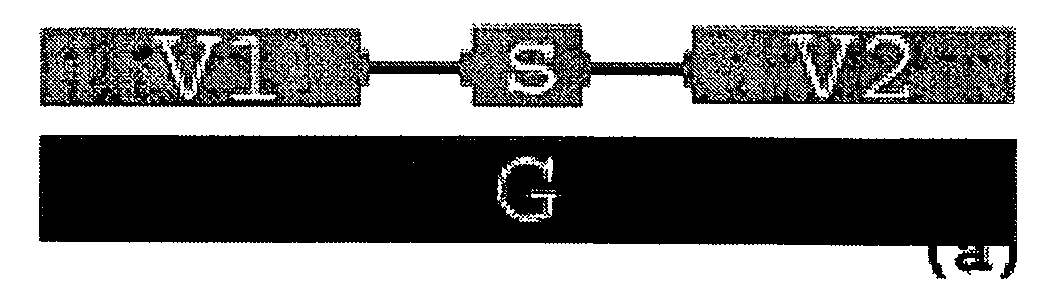
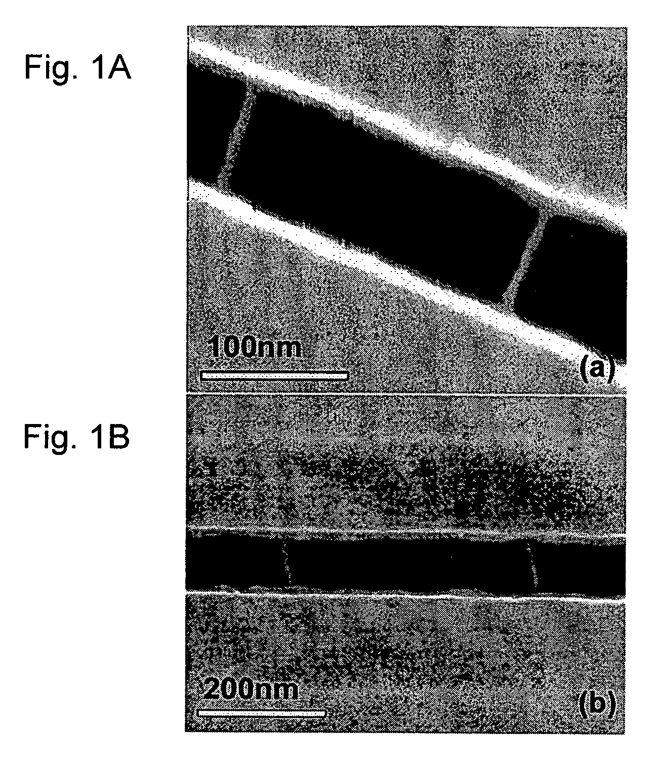
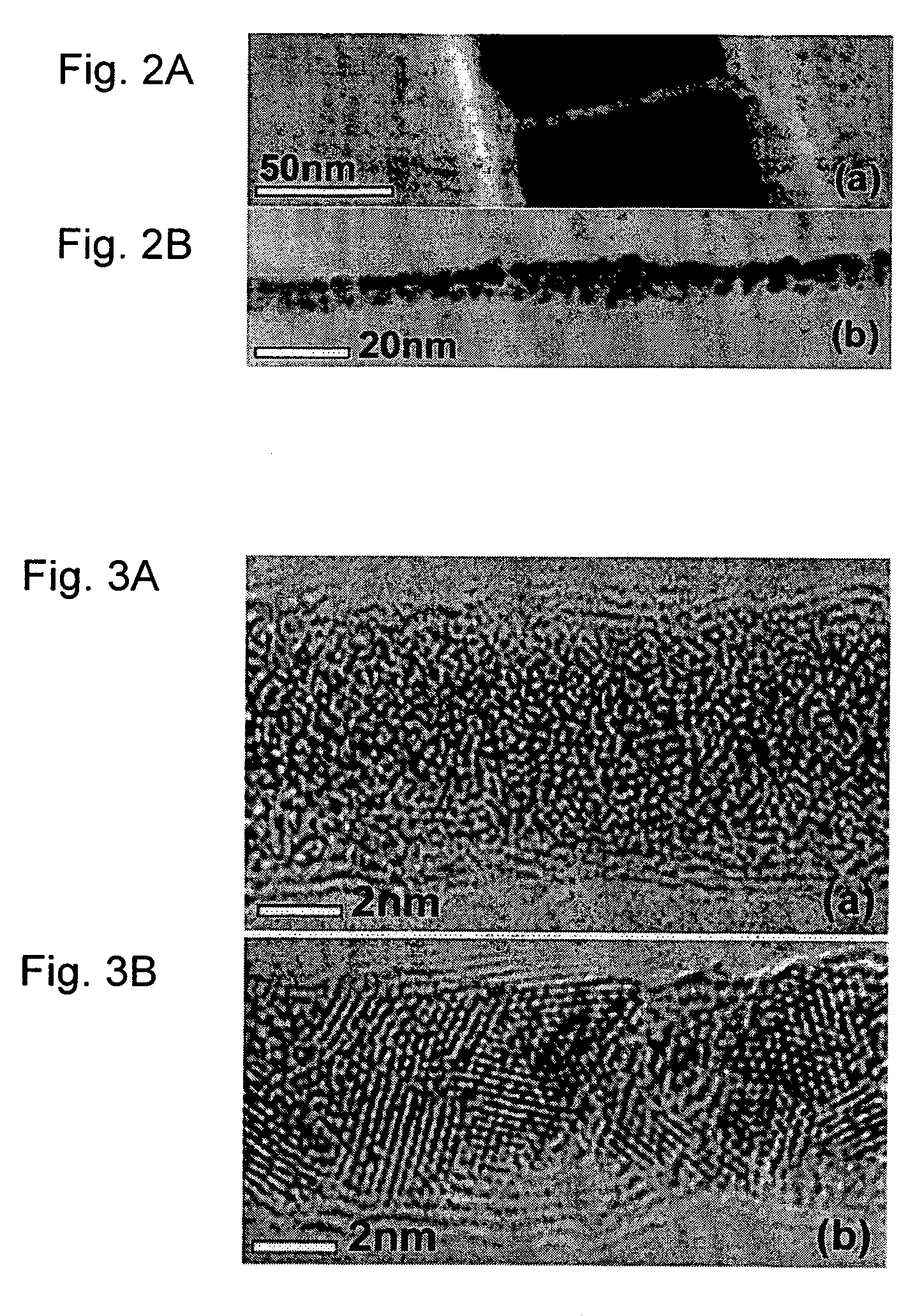
[0063]FIG. 11 shows a SEM (scanning electron microscope) micrograph of a nanowire structure of the present invention. Nanowires of this example were fabricated using single walled carbon nanotube molecular templates, which were posit...


PUM

PropertyMeasurementUnit
diameteraaaaaaaaaa
thicknessaaaaaaaaaa
thicknessaaaaaaaaaa

Abstract

The present invention provides structures and devices comprising conductive segments and conductance constricting segments of a nanowire, such as metallic, superconducting or semiconducting nanowire. The present invention provides structures and devices comprising conductive nanowire segments and conductance constricting nanowire segments having accurately selected phases including crystalline and amorphous states, compositions, morphologies and physical dimensions, including selected cross sectional dimensions, shapes and lengths along the length of a nanowire. Further, the present invention provides methods of processing nanowires capable of patterning a nanowire to form a plurality of conductance constricting segments having selected positions along the length of a nanowire, including conductance constricting segments having reduced cross sectional dimensions and conductance constricting segments comprising one or more insulating materials such as metal oxides.

Description

CROSS REFERENCE TO RELATED APPLICATIONS[0001]This application claims priority under 35 U.S.C. 119(e) to U.S. provisional Patent Application 60 / 678,115 filed May 5, 2005, which is hereby incorporated by reference in its entirety to the extent not inconsistent with the disclosure herein.STATEMENT REGARDING FEDERALLY SPONSORED RESEARCH OR DEVELOPMENT[0002]This invention was made, at least in part, with United States governmental support awarded by Department of Energy Grant DEFG02-91ER45439 and National Science Foundation Grant DMR01-34770. The United States Government has certain rights in this invention.BACKGROUND OF INVENTION[0003]The development of new techniques and processing methods for manipulating, organizing and integrating matter on the scale of nanometers is critically important to continued advances in the field of nanotechnology. These advances are expected to widely impact fundamental and applied technology areas ranging from materials science and physics to applied engi...

Claims


Application Information

Patent Timeline
Patent Type & Authority Patents(United States)
IPC IPC(8): H01L29/76
CPCB82Y10/00H01L29/0673H01L29/7613H01L39/228H01L49/006H01L51/0508H01L51/0048Y10S977/936Y10S977/938Y10S977/937H10N60/128H10N99/05H10K85/221H10K10/46
Inventor BEZRYADIN, ALEXEYREMEIKA, MIKAS
Owner THE BOARD OF TRUSTEES OF THE UNIV OF ILLINOIS
Why Eureka
Try Eureka