Method for forming inorganic silazane-based dielectric film

a dielectric film and inorganic silazane technology, applied in the field of silazane-containing dielectric film, can solve the problems of increasing the tendency of the film to become sparse in the embedded area, peeling or breaking, and increasing the tendency of the film to become spars

Active Publication Date: 2010-08-24
ASM JAPAN
View PDF36 Cites 337 Cited by
  • Summary
  • Abstract
  • Description
  • Claims
  • Application Information

AI Technical Summary

Benefits of technology

[0008]As a process to enable embedding of a film into finer structures, an embodiment of the present invention forms fluid silazane containing no water on a silicon substrate based on a material such as SiH4 or Si2H6 and a nitrogen additive such as NH3 or N2. In an embodiment of the present invention, the susceptor temperature is controlled to a range of −50 to 50° C., and a material such as SiH4 or Si2H6 and a nitrogen additive such as NH3 or N2 are added to form silazane on a silicon substrate by means of plasma CVD. The low susceptor temperature ensures fluidity, and the surface tension enables embedding of a film in patterns having trenches and holes. Also, the reactant gas does not contain oxygen, which means that the generated product does not contain water.
[0010]In an embodiment of the present invention, silazane is dissolved by adding CxHy to add fluidity, which enables embedding of a film regardless of the wiring width. In an embodiment of the present invention, a formed film is UV-cured or heat-treated at 450° C. or above in an oxidizing gas atmosphere to substitute the nitrogen groups in the film with oxygen groups and therefore achieve a dense oxide film. The only substance discharged during heat treatment is the remnant of CxHy that had served as a catalyst in the dissolution of silazane, and accordingly the achieved film has a different contraction coefficient than any liquid material constituted by Si—O and hydrocarbons. As a result, in an embodiment of the present invention the film contraction coefficient is improved significantly to as low as approx. 10% from approx. 30% achieved by conventional methods. The method for forming an oxide film according to the aforementioned embodiment can be effectively applied to any embedded oxide film such as a STI (Shallow Trench Isolation) or PMD (Premetal Dielectric) film.
[0011]There are two methods that provide a function equivalent to the formation of a silazane film using SixHy and NxHy, including a method to form a silazane film offering fluidity by combining SiaNbCdHe (where a, b, d and e are arbitrary integers), and a method to form a silazane film using SiaNbCdHe (where a, b, d and e are arbitrary integers) and then add fluidity by dissolving the formed film in a hydrocarbon gas. Both methods can achieve results equivalent to what can be attained by the aforementioned approach of forming a silazane film using SixHy and NxHy and adding fluidity using a hydrocarbon gas. For your information, these methods can provide a pure oxide film once heat treatment is applied.

Problems solved by technology

However, combination of film formation and etch-back will not likely support smaller device nodes of 60 nm and below, and there is a need for an insulation film offering sufficient filling characteristics in line with the accelerating trend for super-fine circuitry.
However, an oxide film embedded by any such method presents the problems of the film becoming sparse in the embedded area and peeling off or breaking due to change in stress.
Also, water production in the film forming process creates voids when water is subsequently removed in the annealing of the formed film, which also increase the tendency of the film becoming sparse.

Method used


Image

  • Method for forming inorganic silazane-based dielectric film
  • Method for forming inorganic silazane-based dielectric film
  • Method for forming inorganic silazane-based dielectric film

Examples


example

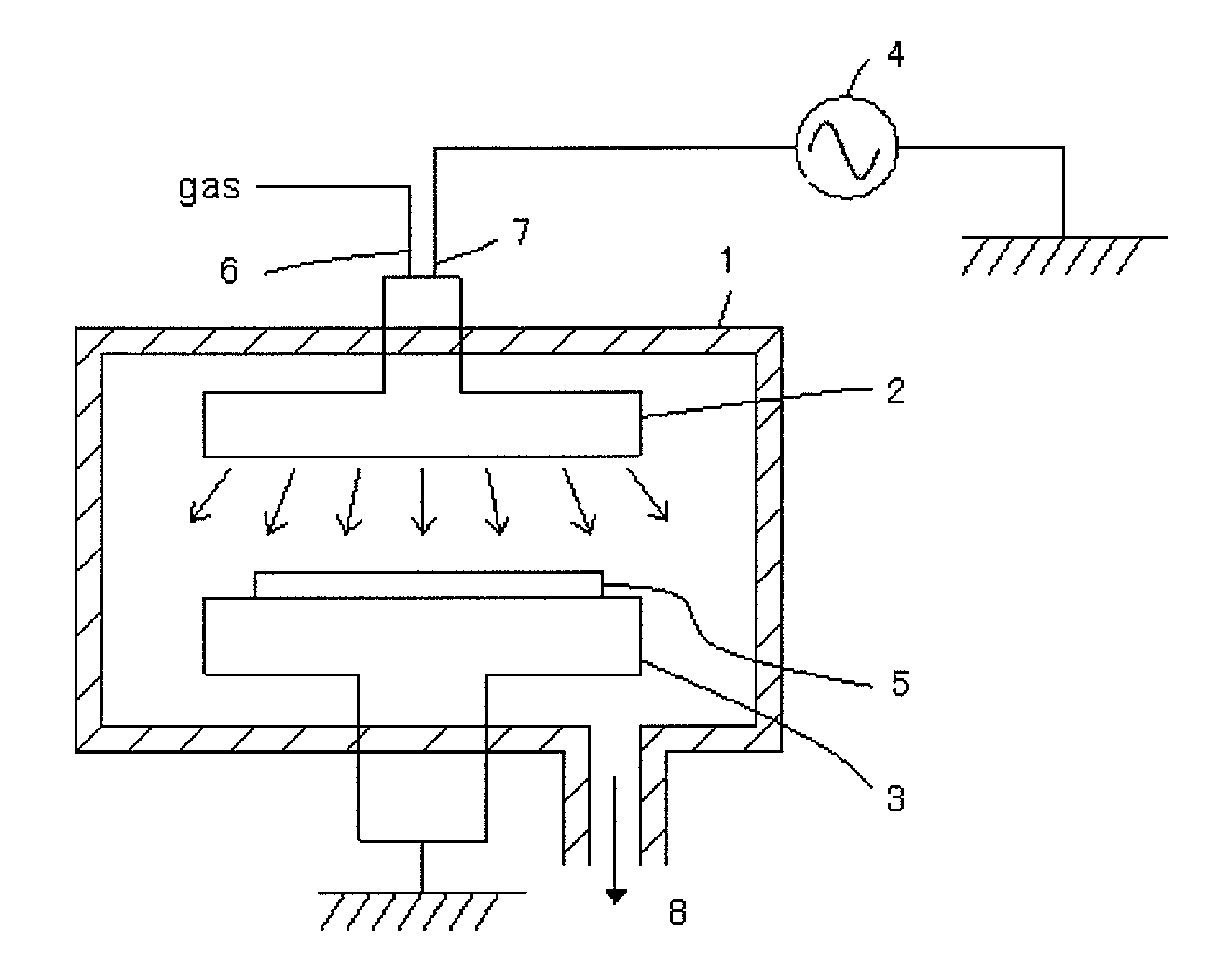
[0091]Experiments were conducted as described below. The results are indicated in tables below. In these experiments, a plasma CVD device shown in FIG. 1 and FIG. 3 was used as an experimental device.

[0092]The diameter of a substrate was 200 mm. The thickness of each insulation film was set at 500 nm.

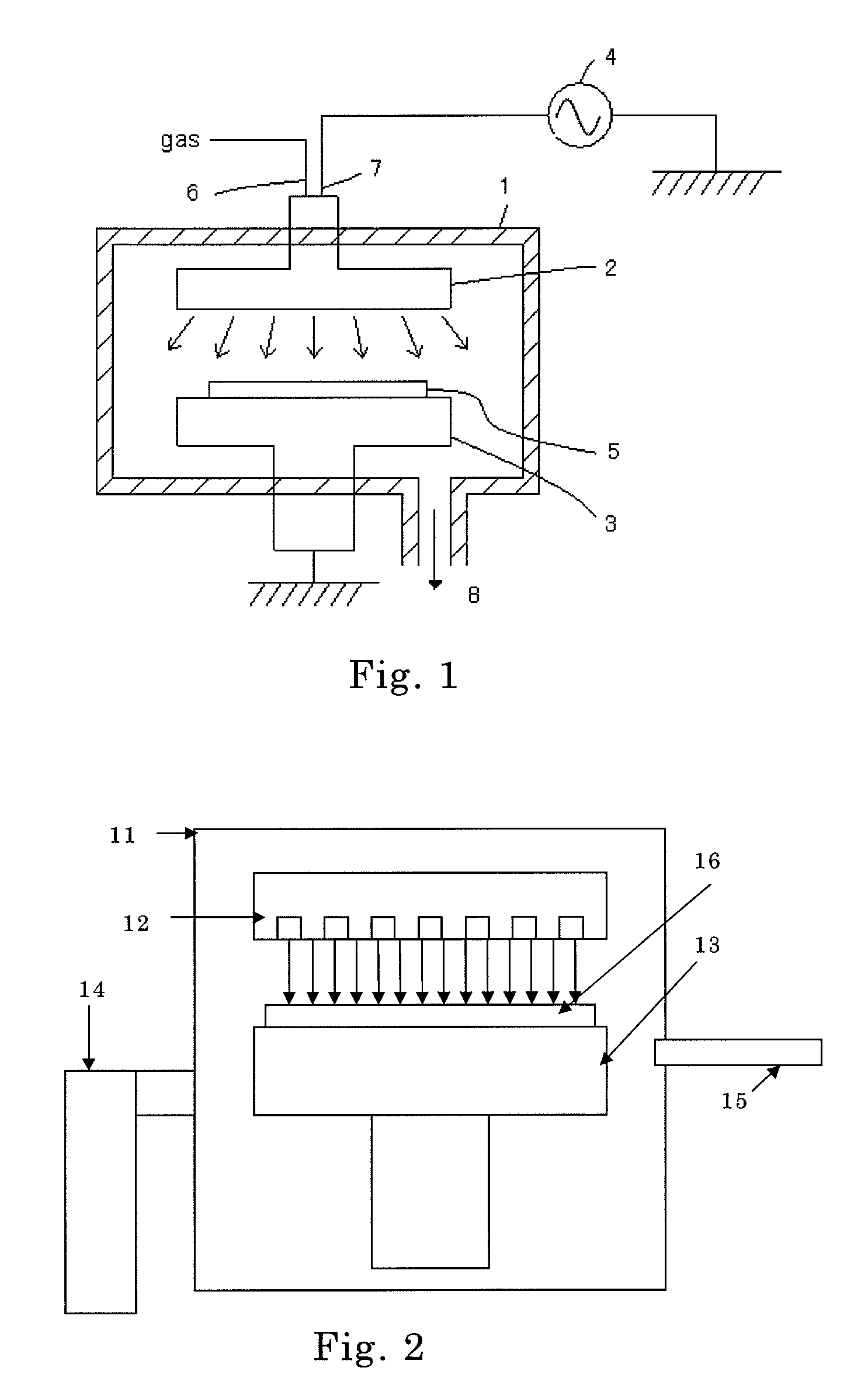
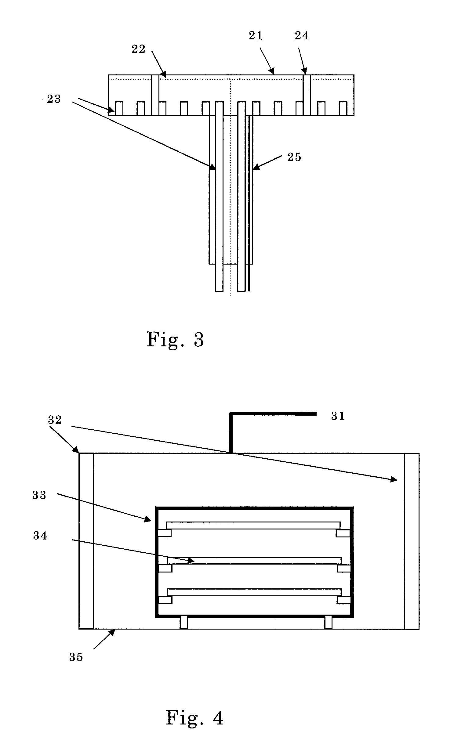
[0093]An insulation film was formed on and filled in an irregular surface of SiN formed on a Si wafer including a hole having a width of 60 nm and a depth of 600 nm. Annealing was conducted in a UV irradiation apparatus shown in FIG. 2 or in a furnace chamber shown in FIG. 4 made of a quartz tube provided with a quartz boat capable of performing annealing at a vacuum pressure to atmospheric pressure.

[0094]Film Formation

Conventional Example

[0095]A low-k film (siloxane film) was formed on a substrate under the conditions shown in Table 1 below.

[0096]

TABLE 1Conventional FormationConventional FormationTriethoxysilane (sccm)10Hexane (sccm)150O2 (sccm)500He (sccm)630Pressure (Pa)266RF (13.56 ...

examples 1-4

[0097]In each example, an inorganic silazane bulk film was first formed on a substrate under the conditions shown in Table 2 below, and then the bulk film was treated with CxHy gas under the conditions shown in Table 3.

[0098]

TABLE 2Silazane Bulk FormationEx. 1Ex. 2Ex. 3Ex. 4SiH4 (sccm)1010050100NH3 (sccm)50255025Ar (sccm)1000100010001000Pressure (Pa)266266266266RF (13.56 MHz) (W)100100100100Susceptor Temp. (° C.)0000Gap (mm)24242424Time (second)60756475

[0099]

TABLE 3CxHy TreatmentEx. 1Ex. 2Ex. 3Ex. 4Hexane (sccm)150150150150Ar (sccm)630630630630Pressure (Pa)2662662661000RF (13.56 MHz) (W)200200200200Susceptor Temp. (° C.)0000Gap (mm)24242424Time (second)95959525

examples 5-8

[0100]In each example, an inorganic silazane bulk film was formed on a substrate with CxHy gas under the conditions shown in Table 4 below.

[0101]

TABLE 4Liquid Layer Formation by SiH4 + NH3 + CxHyEx. 5Ex. 6Ex. 7Ex. 8SiH4 (sccm)1010050100NH3 (sccm)50255025CxHy (sccm)HexaneHexaneHexaneMesitlyene200200200150Ar (sccm)1000100010001000Pressure (Pa)266266266266RF (13.56 MHz) (W)100100100100Susceptor Temp. (° C.)0000Gap (mm)24242424Time (second)55715849

[0102]Heat-Treatment (Post Film Formation)

[0103]Heat-treatment was performed to each film formed on the substrate under the conditions shown in Table 5 below.

[0104]

TABLE 5Post Formation TreatmentSubstrateTemp.DurationIntroducedGas flowPressureCuring type(° C.)(min)gas(sccm)(Pa)Comp.Thermal80060N21000AtmosphericannealingEx. 1↓↓↓O21000↓Ex. 2↓↓↓↓↓↓Ex. 3↓↓↓↓↓↓Ex. 4UV curing40030↓↓1000Ex. 5Thermal80060↓↓AtmosphericannealingEx. 6↓↓↓↓↓↓Ex. 7↓↓↓↓↓↓Ex. 8↓↓↓↓↓↓

[0105]Film Characteristics

[0106]Each thus-obtained film was evaluated and the results are show...


PUM

PropertyMeasurementUnit
temperatureaaaaaaaaaa

Abstract

A method of forming an inorganic silazane-based dielectric film includes: introducing a gas constituted by Si and H and a gas constituted by N and optionally H into a reaction chamber where an object is placed; controlling a temperature of the object at −50° C. to 50° C.; and depositing by plasma reaction a film constituted by Si, N, and H containing inorganic silazane bonds.

Description

BACKGROUND OF THE INVENTION[0001]1. Field of the Invention[0002]The present invention relates generally to a semiconductor technique and more particularly to a silicone-containing dielectric film having good filling or padding property for an interconnect structure of a semiconductor substrate.[0003]2. Description of the Related Art[0004]In the plasma chemical vapor deposition method (plasma CVD method), deposition of a film on semiconductor substrates is conducted by placing each semiconductor substrate, being a processing target, on a resistance-heating type heater preheated to 0 to 350° C. in an atmosphere of 1 to 10 Torr. This heater is placed in a manner facing a shower plate that releases reactant gas, and high-frequency power of 13.56 MHz to 60 MHz, etc., is applied by 100 to 4,000 W to the shower plate to cause high-frequency discharge between the heater and shower plate and thereby generate plasma. The plasma CVD method is used to deposit various types of thin film, such as...

Claims


Application Information

Patent Timeline
Patent Type & Authority Patents(United States)
IPC IPC(8): H01L21/31H01L21/469
CPCH01L21/02211H01L21/02274H01L21/02326H01L21/02337H01L21/02348C23C16/34C23C16/345C23C16/505H01L21/02164H01L21/0217C23C16/30C23C16/00
Inventor FUKAZAWA, ATSUKIMATSUKI, NOBUOHA, JEONGSEOK
Owner ASM JAPAN
Why Eureka
Try Eureka