Optical data latch

a technology of optical information and latches, applied in logic circuits, cladded optical fibres, instruments, etc., can solve the problems of undesirable asynchronous operation, prior digital optical logic gates are incapable of storing optical information being processed, etc., and achieve the effect of increasing the operating speed

Active Publication Date: 2010-08-31
NAT TECH & ENG SOLUTIONS OF SANDIA LLC
View PDF2 Cites 7 Cited by
  • Summary
  • Abstract
  • Description
  • Claims
  • Application Information

AI Technical Summary

Benefits of technology

[0009]The present invention relates to an optical data latch which comprises a pair of optical logic gates, with each optical logic gate comprising a waveguide electroabsorption modulator which is electrically connected in series with a waveguide photodetector which has one or more photodetector inputs. Each optical logic gate has a modulator input wherein light is coupled into the waveguide electroabsorption modulator, with the light which is transmitted through the waveguide electroabsorption modulator forming an output for that optical logic gate. In the optical data latch, a plurality of optical waveguides are used to connect the pair of optical logic gates in a cross-coupled arrangement wherein the output of each optical logic gate of the pair of optical logic gates is optically connected to one of the photodetector inputs of the ot

Problems solved by technology

Prior digital optical logic gates have been incapable of storing the optical information being processed and thus have operated asynchronously.
Such asynchronou

Method used


Image

  • Optical data latch
  • Optical data latch
  • Optical data latch

Examples


Embodiment Construction

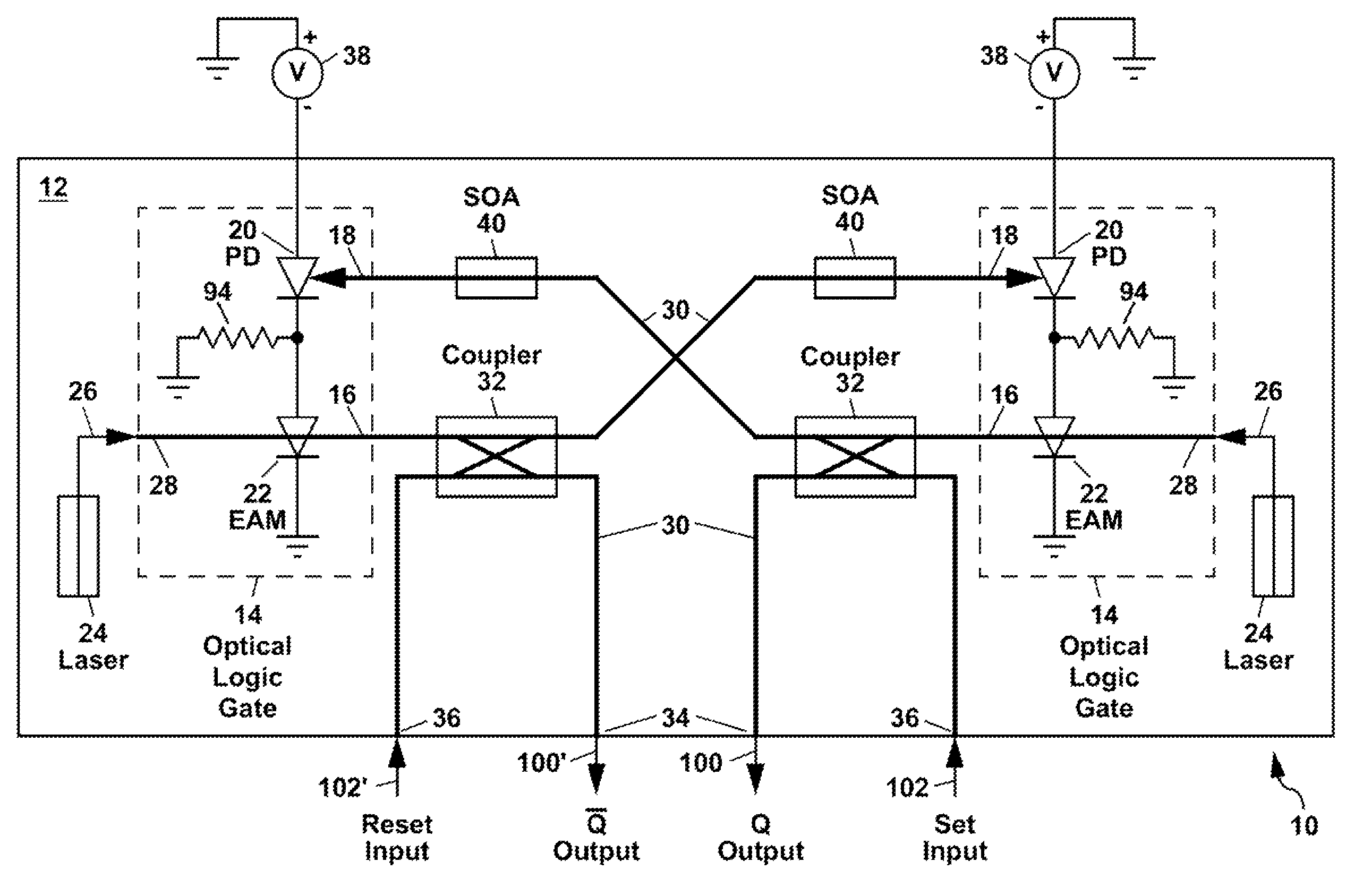
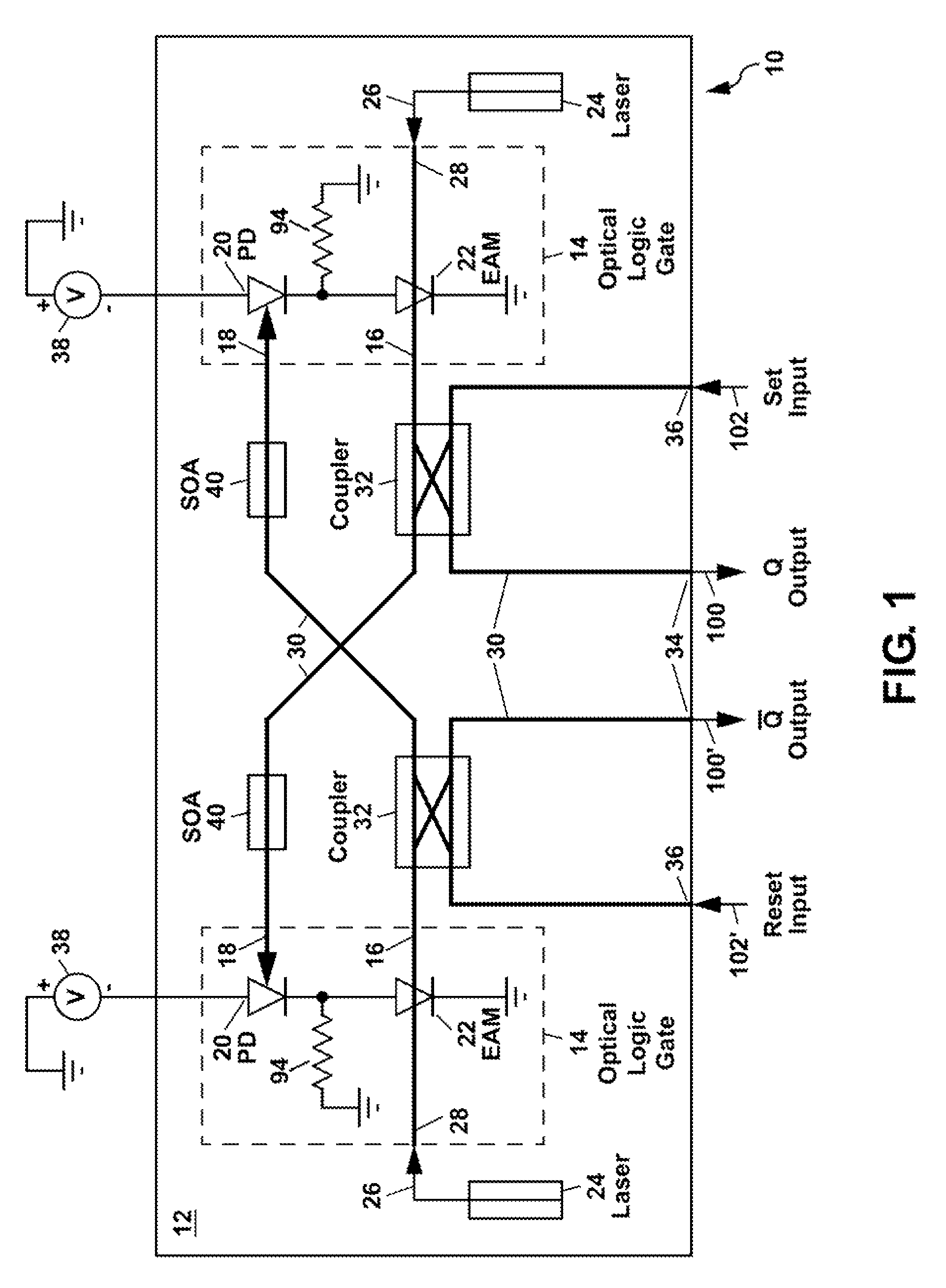
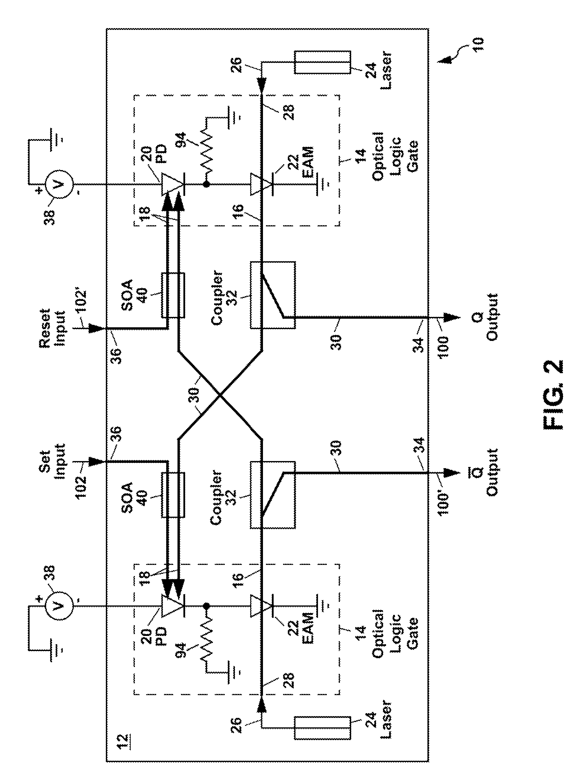
[0033]Referring to FIG. 1, there is shown a schematic diagram of a first example of the optical data latch 10 of the present invention which can be formed as a photonic integrated circuit (PIC). The optical data latch 10 comprises a substrate 12 on which are formed a pair of optical logic gates 14 which are connected in a cross-coupled arrangement whereby an output 16 of each optical logic gate 14 is optically connected to a photodetector input 18 of the other optical logic gate 14. This cross-coupled arrangement of the two optical logic gates 14 forms a bi-stable optical feedback loop which forces the outputs 16 of the pair of optical logic gates 14 to be exactly opposite of each other so that when one output 16 is bright (i.e. having a relatively high level of light which corresponds to a logical “1” state), then the other output 16 will be dark (i.e. having little or no light which corresponds to a logical “0” state). In this way, the optical data latch 10 can store a bit of opti...


PUM


Abstract

An optical data latch is formed on a substrate from a pair of optical logic gates in a cross-coupled arrangement in which optical waveguides are used to couple an output of each gate to an photodetector input of the other gate. This provides an optical bi-stability which can be used to store a bit of optical information in the latch. Each optical logic gate, which can be an optical NOT gate (i.e. an optical inverter) or an optical NOR gate, includes a waveguide photodetector electrically connected in series with a waveguide electroabsorption modulator. The optical data latch can be formed on a III-V compound semiconductor substrate (e.g. an InP or GaAs substrate) from III-V compound semiconductor layers. A number of optical data latches can be cascaded to form a clocked optical data shift register.

Description

GOVERNMENT RIGHTS[0001]This invention was made with Government support under Contract No. DE-AC04-94AL85000 awarded by the U.S. Department of Energy. The Government has certain rights in the invention.CROSS REFERENCE TO RELATED APPLICATIONS[0002]The present application is related to U.S. patent application Ser. No. 12 / 182,683, entitled “Optical NAND Gate,” of common assignee filed on Jul. 30, 2008, the contents of which are incorporated herein by reference in their entirety. The present application is also related to U.S. patent application Ser. No. 12 / 270,221, entitled “Optical NOR Gate,” of common assignee filed on Nov. 13, 2008, the contents of which are incorporated herein by reference in their entirety.FIELD OF THE INVENTION[0003]The present invention relates in general to digital optical logic, and in particular to a optical data latch which utilizes waveguide electroabsorption modulators and waveguide photodetectors to store optical information. The optical data latch can als...

Claims


Application Information

Patent Timeline
IPC IPC(8): G02B6/12
CPCH03K3/42H03K19/14H03K19/20
Inventor VAWTER, G. ALLEN
Owner NAT TECH & ENG SOLUTIONS OF SANDIA LLC
Why Eureka
Try Eureka