Selective electrochemical accelerator removal

a selective electrochemical and accelerator technology, applied in the manufacture of electrolysis components, printed circuits, manufacturing tools, etc., can solve the problems of requiring significant excess metal deposition, requiring “overburden”, and low aspect ratio features that lose all metal below the dielectric plane. , to achieve the effect of reducing the extent of overplating, reducing the thickness of excess electroplating, and high aspect ratio

Active Publication Date: 2010-09-21
NOVELLUS SYSTEMS
View PDF72 Cites 32 Cited by
  • Summary
  • Abstract
  • Description
  • Claims
  • Application Information

AI Technical Summary

Benefits of technology

[0015]Aspects of the present invention relate to methods of preferentially filling by electroplating features that are recessed from the general plane of a workpiece. Aspects of the invention relate to 1) a process for improving the filling high aspect ratio (features deeper than wide) recess features, 2) the reduction of excess electroplating thickness commonly observed during copper electrodeposition over high aspect ratio feature (a “mound” or “bump” or excessive metal often found after filling high aspect ratio features, sometimes called “momentum” or “overplating”), and 3) the preferential filling with metal (referred to hereafter as “bottom-up” filling or selective accelerated plating) in recessed area of a surface of low aspect ratio damascene features (features much wider than deep). The invention is thus applicable, for example, to the manufacture of integrated circuit or other electronic devices. Aspects of the invention further relate to hardware for performing and controlling these processes, reducing the extent of overplating, providing selective accelerated plating and preferentially filling high and low aspect ratio damascene features. In addition, the invention relates to removal of excess metal, specifically the metal from the general planar surface of a workpiece. In certain embodiments, each of these deposition and removal steps occurs primarily though electrochemical action rather than, for example, physical abrasion, sputtering, etc. In some embodiments these steps are performed with little or no physical contact with the surface of the workpiece under construction at any time. In some cases it has been found useful to continue the feature filling process beyond the simple filling of the recesses to a point were raised, inverted, or “embossed” regions are created over underlying features. The protecting of the underlying structure with excess metal can reduce undercutting, dishing, and erosion as well as the potential adverse impact on the underlying topography caused by subsequent device level manufacture and the dielectric planarization steps (e.g., barrier / dielectric CMP). In such instances to later remove the overfill, additional removal process sequences may be used, such as a non-contacting wet etch (such as an isotropic wet etch) or membrane mediated electropolishing.

Problems solved by technology

For the most part, prior processes do not preferentially fill and planarize low aspect ratio features and therefore they require significant excess metal deposition (“overburden”).
However if metal was subsequently isotropically removed, then these low aspect ratio features would lose all the metal below the plane of the dielectric before the high aspect ratio lines and field area metal was removed.
But to use these polishing planarizing technologies, “overburden” is required.
Overburden is undesirable for a number of reasons.
Thus, overburden represents additional materials costs (excess copper deposited and removed) as well as decreased throughput / productivity.
The CMP and eCMP processes are particularly expensive process and implement generally corrosive chemical and slurry formulations on large pads to polish the surface of the integrated circuit.
Polishing can be difficult to control and the polishing end-point can be difficult to detect.
The high equipment cost, waste handling cost, and low throughput contribute to the overall expense of CMP and eCMP.
Also, with the introduction of porous low-k dielectrics in semiconductor devices, modification of traditional CMP and even eCMP processes will be required, as current methods can lead to cracking and / or delamination of low-k materials which are fragile and typically have a very low compression strength.
Because neither the metal deposition (e.g., electroplating) nor metal removal (e.g., CMP) processes are perfectly uniform across the wafer surface, global non-uniformities also exist.
The problem arises that the interconnect metal (e.g., copper) in the feature is slowly removed, preferentially within the feature, hence it becomes “dished”.
Varying feature density and the different mechanical properties of the metal and dielectric are the leading causes of polishing erosion.
The overall changes in the planarity caused by dishing, erosion, and underlying topography can also lead to difficulties in obtaining good focus across the die during subsequent lithographic steps.
These areas are particularly troublesome for CMP technology because of the competing requirements of having planarization and compliance.
Clearing metal by CMP from recessed areas of “underlying topography is difficult, often leaving “puddles” of metal.
To remove these “puddles,” the CMP process is generally continued for a longer period of time than otherwise desirable because it can create excessive dishing.
These issues make CMP progressively more difficult with advancing technology requiring additional numbers of metal layers to be added to the structure.
However, the physical and geometrical limitations of these processes, mean that they are not capable of filling low aspect ratio features Since both high and low aspect ratio features can exist on every damascene integrated circuit interconnect level, there is interest in any potentially low cost “planar plating” method.

Method used


Image

  • Selective electrochemical accelerator removal
  • Selective electrochemical accelerator removal
  • Selective electrochemical accelerator removal

Examples


example

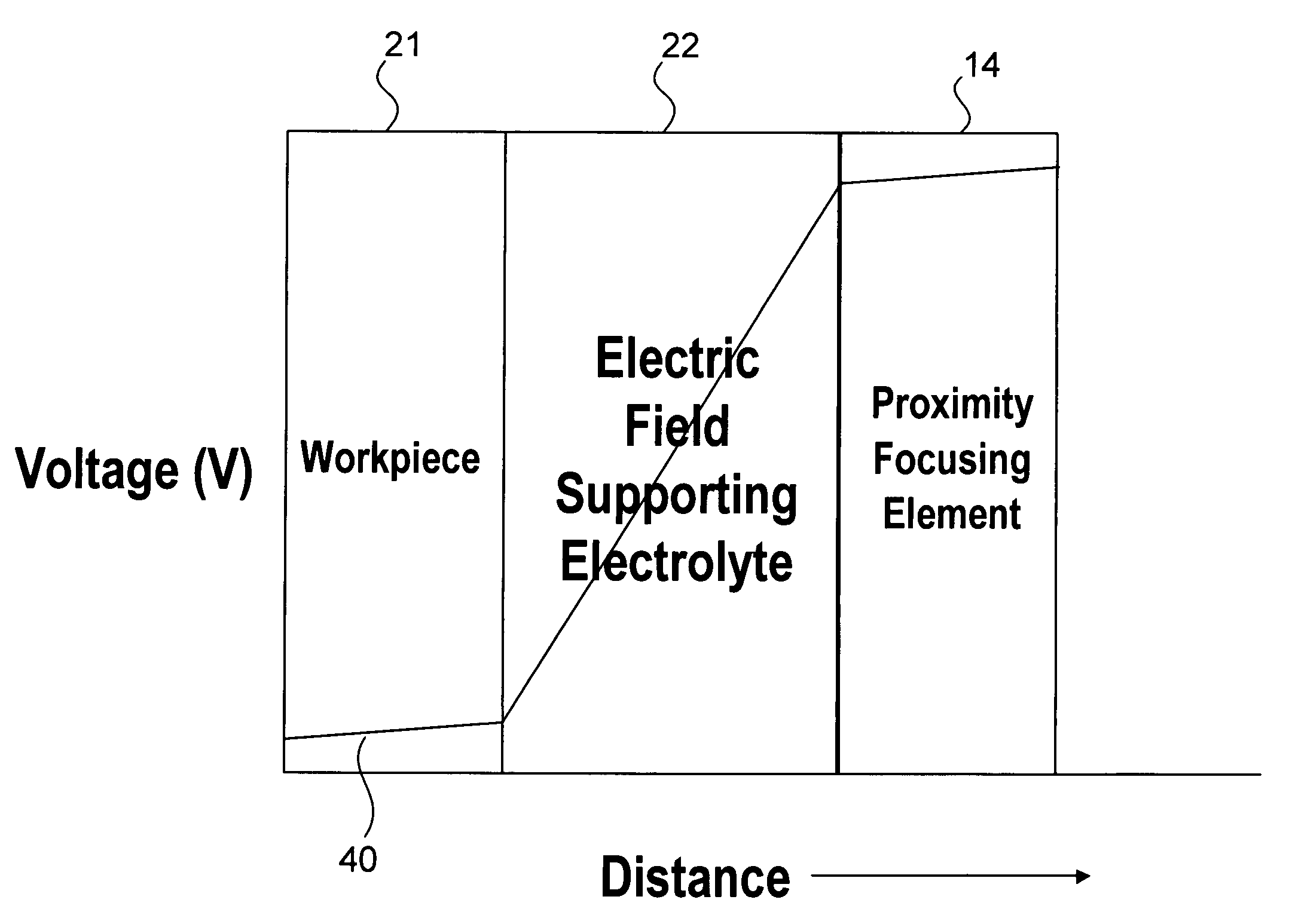
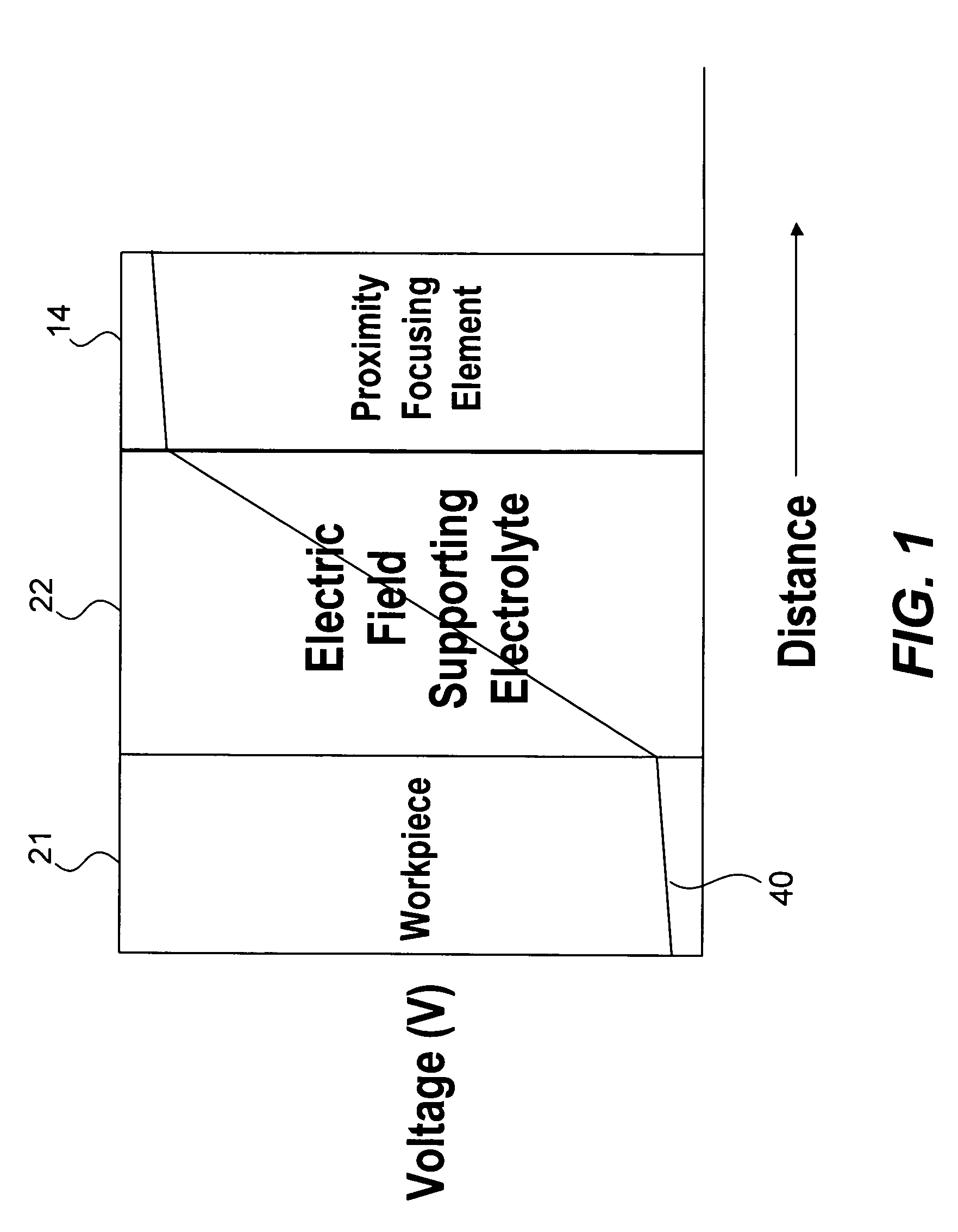
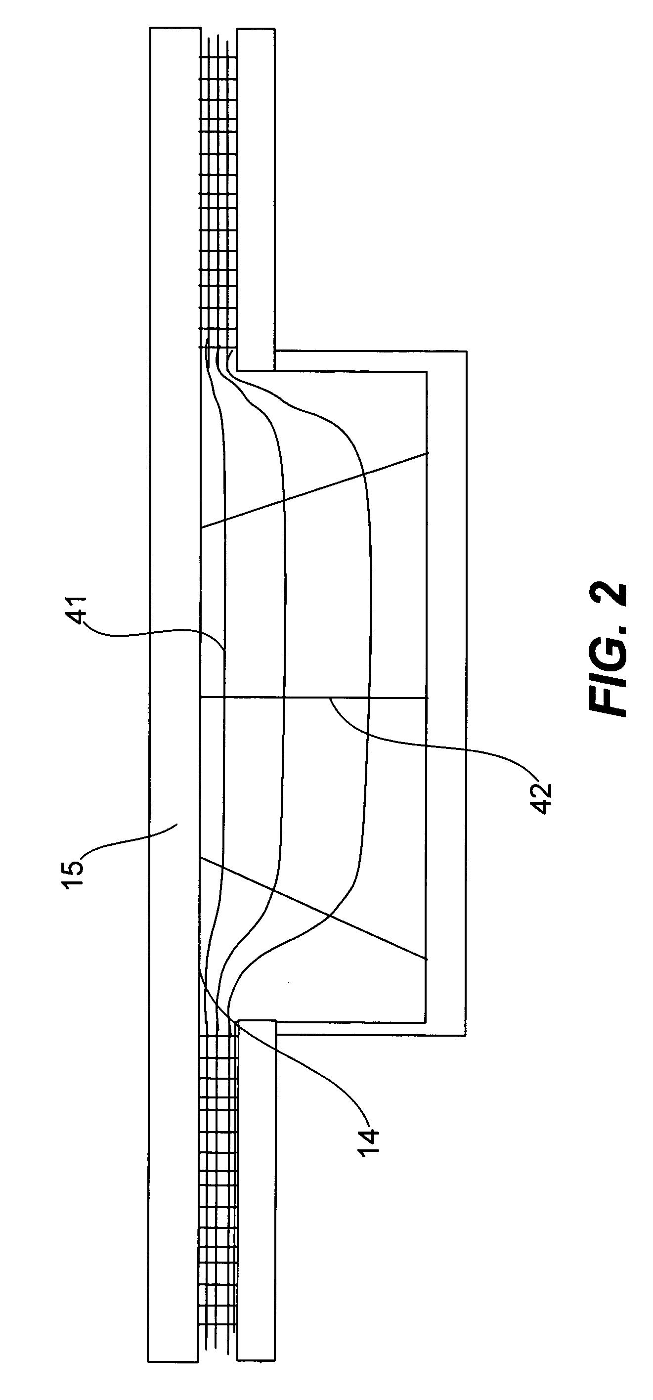
[0101]The procedure to achieve these results is now described, but we are not implying that this is the only procedure or the optimal procedure. A 200 mm wafer was first sprayed with deionized wafer to wet the surface for 3 seconds, then sprayed with a 5% solution of sulfuric acid for 5 seconds to remove a surface oxide, followed by rinsing with a spray of DI water to remove the acid, followed by spraying with a solution containing 1 g / L MPSA in water for 10 seconds to uniformly accelerated the wafer. The wafer was then rinsed completely with water and then dried in air by spinning the wafer at 1500 rpm at about 20° C. (Despite rinsing and drying, the accelerant still remains attached to the surface). Next a SMMART EFIE head was passed over the surface at 50 cm / sec. The velocity was maintained constant by varying the rotation rate as a function of radial position of the head. Pure deionized water was used as an electric field supporting electrolyte. An approximately one molar soluti...


PUM

PropertyMeasurementUnit
electric fieldaaaaaaaaaa
electric field strengthaaaaaaaaaa
areaaaaaaaaaaa

Abstract

Methods and apparatus are provided for planar metal plating on a workpiece having a surface with recessed regions and exposed surface regions; comprising the steps of: causing a plating accelerator to become attached to said surface including the recessed and exposed surface regions; selectively removing the plating accelerator from the exposed surface regions without performing substantial metal plating on the surface; and after removal of plating accelerator is at least partially complete, plating metal onto the surface, whereby the plating accelerator remaining attached to the surface increases the rate of metal plating in the recessed regions relative to the rate of metal plating in the exposed surface regions.

Description

CROSS-REFERENCE TO RELATED APPLICATIONS[0001]This application is a continuation-in-part, claiming priority under 35 USC 120 from U.S. patent application Ser. No. 11 / 065,708, filed Feb. 23, 2005, entitled “Method And Apparatus For Uniform Electropolishing of Damascene IC Structures By Selective Agitation” in the names of Mayer et al., now U.S. Pat. No. 7,531,079, which is a continuation-in-part of U.S. patent application Ser. No. 10 / 739,822, filed Dec. 17, 2003, now U.S. Pat. No. 7,449,098, which is in turn a continuation-in-part of U.S. patent application Ser. No. 10 / 209,171, filed Jul. 29, 2002, now U.S. Pat. No. 6,756,307. Each of these applications is incorporated herein by reference in its entirety and for all purposes.[0002]Priority is claimed under 35 USC 119(e) from U.S. Provisional Patent Application Ser. No. 60 / 724,209, filed Oct. 5, 2005, which is incorporated by reference in its entirety and for all purposes.[0003]This application is also a continuation-in-part of U.S. Se...

Claims


Application Information

Patent Timeline
Patent Type & Authority Patents(United States)
IPC IPC(8): C25F3/00H01L21/288B23H3/00
CPCB23H5/08C25F3/16H01L21/7684H01L21/2885H01L21/32115H01L21/02068
Inventor MAYER, STEVEN T.DREWERY, JOHNHILL, RICHARD S.ARCHER, TIMOTHYKEPTEN, AVISHAI
Owner NOVELLUS SYSTEMS
Why Eureka
Try Eureka