Method of manufacturing semiconductor device, method of manufacturing display apparatus, apparatus of manufacturing semiconductor device, and display apparatus
a display apparatus and semiconductor technology, applied in the direction of semiconductor/solid-state device testing/measurement, manufacturing tools, instruments, etc., can solve the problems of accidental tilting of the irradiation optical system, reduced display unevenness in the display apparatus, and visual recognition of the characteristic difference between the crystallinity of the forward path and the crystallinity of the backward path, and achieves reduced characteristic variation in the semiconductor device formed over the semiconductor film. , the effect of reducing the differen
- Summary
- Abstract
- Description
- Claims
- Application Information
AI Technical Summary
Benefits of technology
Problems solved by technology
Method used
Image

Examples
first embodiment
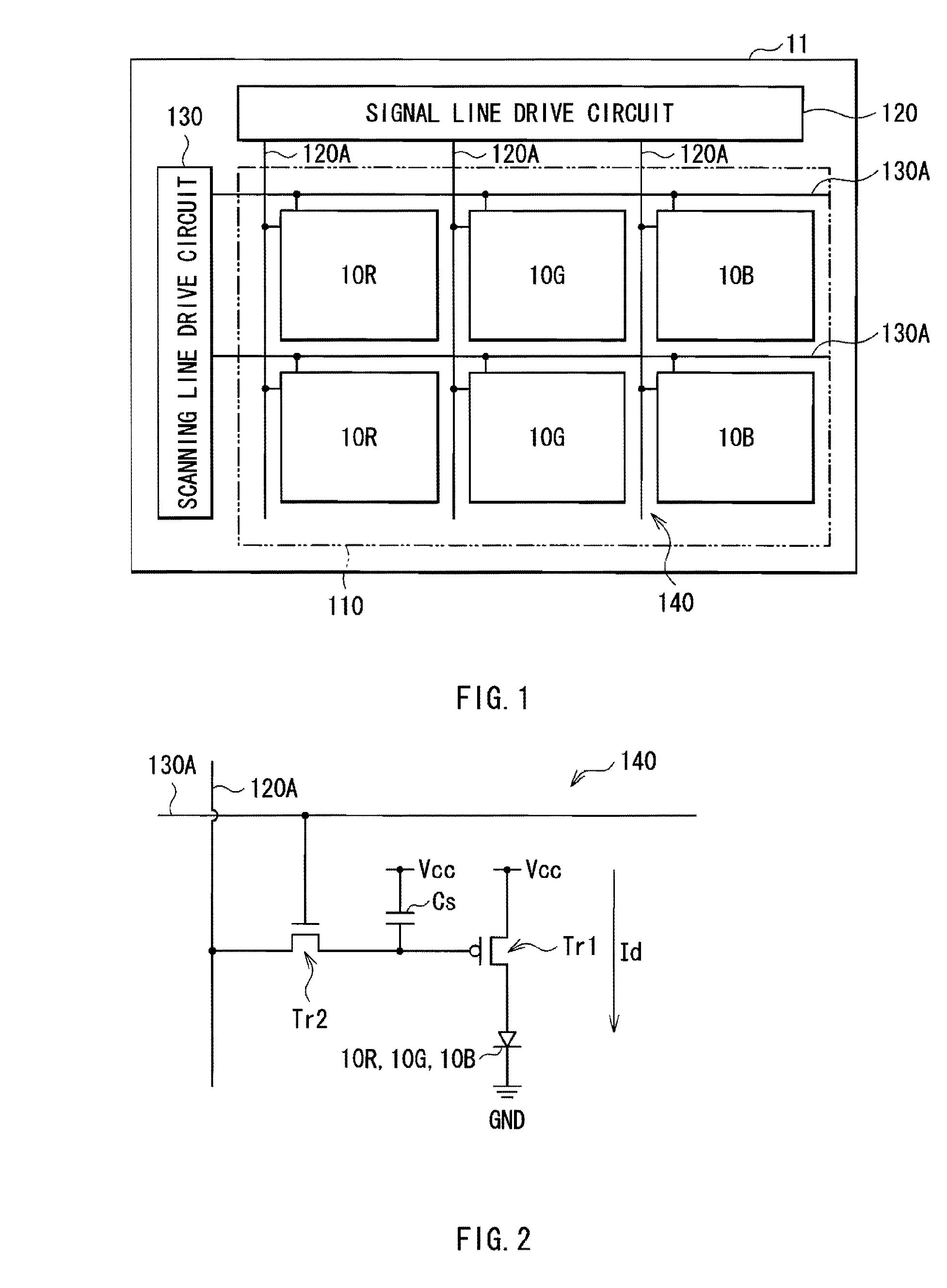
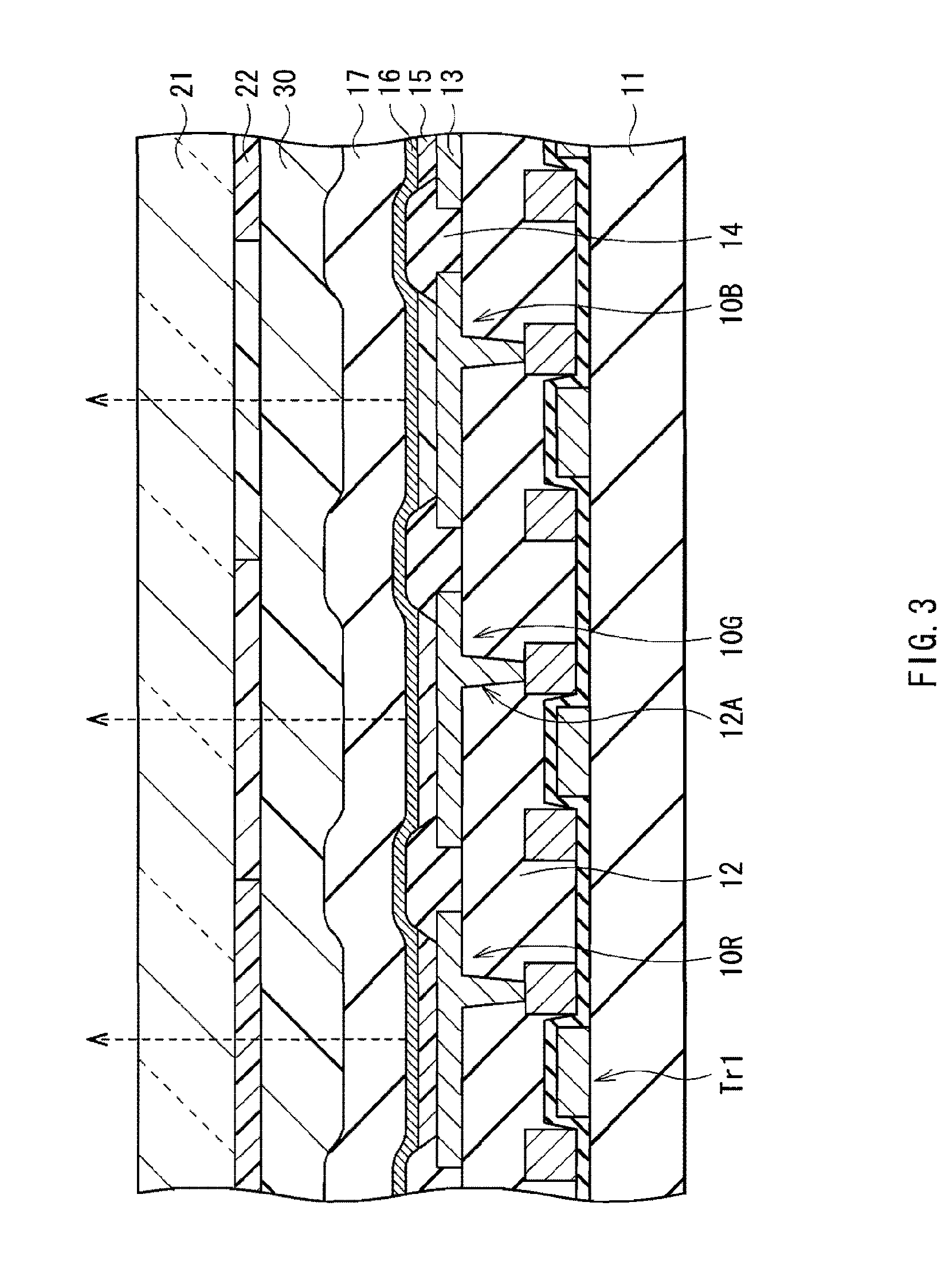
[0048]FIG. 1 shows a configuration of a display apparatus as a first embodiment of the present invention. The display apparatus is used as an ultrathin organic light emitting color display apparatus or the like. For example, a display area 110 in which a plurality of organic light emitting elements 10R, 10G, and 10B which will be described later are disposed in a matrix on a substrate 11 made of glass. Around the display area 110, a signal line drive circuit 120 and a scanning line drive circuit 130 as drivers for displaying a video image are formed.
[0049]A pixel drive circuit 140 is formed in the display area 110. FIG. 2 shows an example of the pixel drive circuit 140. The pixel drive circuit 140 is an active-type drive circuit formed in a layer under a first electrode 15 which will be described later, and having a drive transistor Tr1 and a write transistor Tr2, a capacitor (holding capacitor) Cs between the transistors Tr1 and Tr2, and the organic light emitting element 10R (10G,...
second embodiment
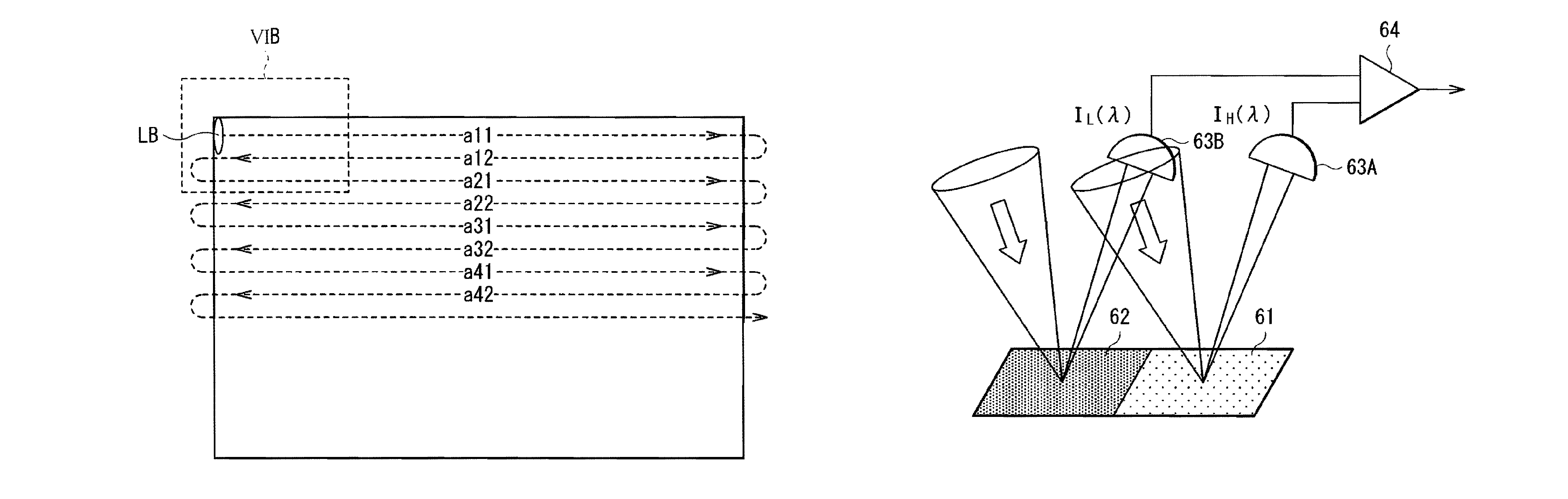
[0093]FIG. 13 is a diagram for explaining a method of manufacturing a display apparatus according to a second embodiment of the invention. In the second embodiment, in place of the irradiation power of the laser beam LB, relative speeds of the laser beam LB and the substrate 11, that is, the speed of the movable stage 51 (stage speed) is modulated. Except for this point, the manufacturing method of the second embodiment is the same as that of the first embodiment. The same operations and effects are obtained. Therefore, the same reference numerals are designated to corresponding elements, and description will be given.
[0094]FIG. 13 shows the relation between stage speed and contrast at certain irradiation powers in the forward path a1 and the backward path a2. FIG. 13 shows the case where the irradiation optical system 53 tilts with respect to the substrate 11 only by the angle φ, or the case where the section profile of the laser beam LB with respect to the plane perpendicular to t...
third embodiment
[0096]FIG. 14 shows a whole configuration of an annealing apparatus used in a third embodiment of the invention. In the third embodiment, by using the annealing apparatus 50 having three sets of the light source 52 and the irradiation optical system 53 (light sources 52A to 52C and irradiation optical systems 53A to 53C) as shown in FIG. 14, the throughput is further increased. However, in the case of moving the laser beam LB and the substrate 11 relative to each other by the movable stage 51, the stage speed may not be modulated independently in each of the irradiation optical systems 53. Consequently, in the third embodiment, the irradiation power of the laser beam LB is modulated in a manner similar to the first embodiment in each of the irradiation optical systems 53. Except for this point, the manufacturing method of the third embodiment is the same as that of the first embodiment, and the operations and effects are also the same. Therefore, the same reference numerals are desi...
PUM
| Property | Measurement | Unit |
|---|---|---|
| thickness | aaaaa | aaaaa |
| thickness | aaaaa | aaaaa |
| thickness | aaaaa | aaaaa |
Abstract
Description
Claims
Application Information
 - R&D
- Intellectual Property
- Life Sciences
- Materials
- Tech Scout
- Unparalleled Data Quality
- Higher Quality Content
- 60% Fewer Hallucinations
Browse by: Latest US Patents, China's latest patents, Technical Efficacy Thesaurus, Application Domain, Technology Topic, Popular Technical Reports.
© 2025 PatSnap. All rights reserved.Legal|Privacy policy|Modern Slavery Act Transparency Statement|Sitemap|About US| Contact US: help@patsnap.com