Heterostructure, injector laser, semiconductor amplifying element and a semiconductor optical amplifier a final stage

a semiconductor optical amplifier and injector laser technology, applied in the field ofquantum electronic engineering, can solve the problems of limiting the possible attainment of higher energy and spatial characteristics, certain degree limiting the attainment of low lasing threshold currents, high efficiency and power, etc., to achieve the effect of improving frequency, speed, spectral and spatial characteristics, and improving energy and spatial characteristics

Inactive Publication Date: 2010-11-23
GENERAL NANO OPTICS
View PDF5 Cites 5 Cited by
  • Summary
  • Abstract
  • Description
  • Claims
  • Application Information

AI Technical Summary

Benefits of technology

[0016]The technical problem of the invention was to modernize the design of the heterostructure, in particular—the leak-in region of emission and the active layer, for achievement of the technical result—the improvement of the energy and spatial characteristics of the semiconductor injection emission sources manufactured on its basis, namely—the creation of the high-power, high-efficiency and highly reliable said emission sources (including single-frequency and single-mode) with the improved frequency, speed, spectral and spatial characteristics, the decreased optical losses, lesser emission divergence angles, improved temperature dependencies of the emission power, decreased non-linear deviations of emission, as well as with the decreased ohmic and heat resistence, decreased level of the mechanical stresses and increased operational resource semiconductor injection emission sources along with the further simplification of technology of manufacturing of heterostructure.
[0017]The technical result of the invention is the further reducing of the lasing threshold currents and the increasing of the efficiency, output power and reliability of the injection laser together with high spatial characteristics of laser emission including the single-mode, single-frequency injection laser, as well as the reducing of ohmic and thermal resistances, the reducing of the level of compressive mechanical stresses, the improving of the distribution of the near and far fields of emission, the improving of the temperature dependences of output parameters, the reducing of the nonlinear distortion of emission contributing not only to obtaining high output powers, but also to decreasing of the width of a emission spectrum line, reduction of its frequency shift, the improvement of high-frequency and high-speed modulation characteristics, as well as the increasing of the operational resource along with the further simplification of technology of manufacturing of the device.
[0018]The technical result of the invention is the increasing of the sensitivity to an input signal and the increasing of the value of coefficient of small-signal amplification of the semiconductor amplifying element as well as the further reduction of the nonlinear distortion of emission for creation of high-power, high-efficiency, highly reliable, low-noise, high-frequency, high-aperture semiconductor optical amplifiers with small angles of divergence of output emission, with improved distribution of the near and far fields of emission, with reduced sensitivity to polarization of input emission, improved temperature dependences, reduced ohmic and thermal resistances, and a reduced level of mechanical stresses, as well as the increasing of operational resource of the semiconductor amplifying element along with the further simplification of technology of manufacturing of the device.

Problems solved by technology

At the same time the said heterostructure limits the possible attainment of higher energy and spatial characteristics of the IES manufactured on its basis.
At the same time the prototype injection laser to a certain degree limits the attainment of low lasing threshold currents, as well as high efficiency and power of laser emission together with its high spatial characteristics.
At the same time the prototype SAE has an insufficient sensitivity to an input signal and certain restrictions on the magnitude of the small-signal amplification coefficient.

Method used


Image

  • Heterostructure, injector laser, semiconductor amplifying element and a semiconductor optical amplifier a final stage
  • Heterostructure, injector laser, semiconductor amplifying element and a semiconductor optical amplifier a final stage
  • Heterostructure, injector laser, semiconductor amplifying element and a semiconductor optical amplifier a final stage

Examples


Embodiment Construction

[0106]Hereinafter the invention is explained by the description of concrete embodiments with references to the enclosed drawings. The given examples of the embodiments of the HS, Laser, SAE, and SOA are not the only ones and assume the availability of other realizations, including the known wavelength ranges, the features of which are reflected in the sum of the distinctions according to the claim.

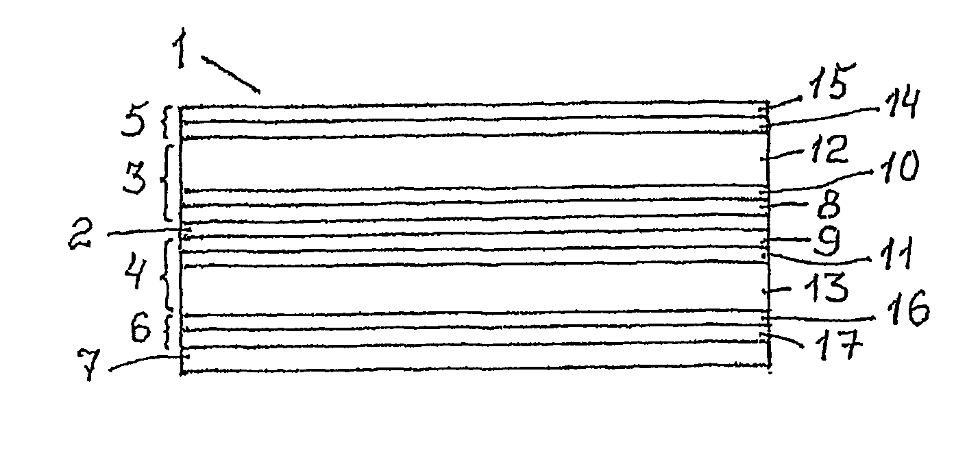
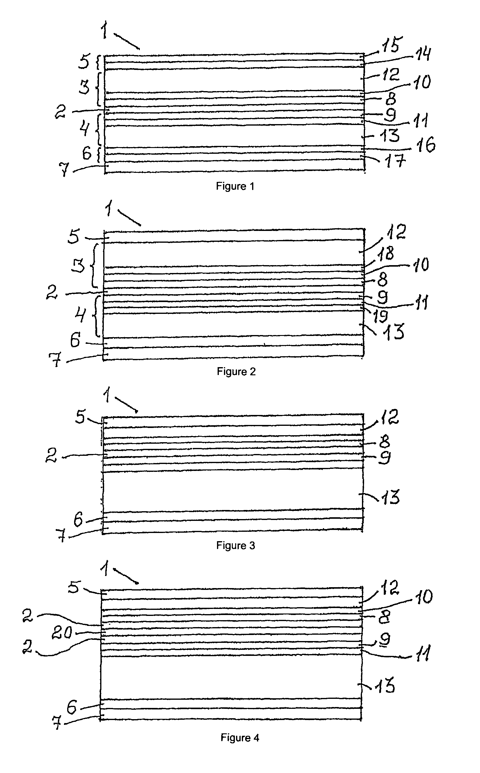
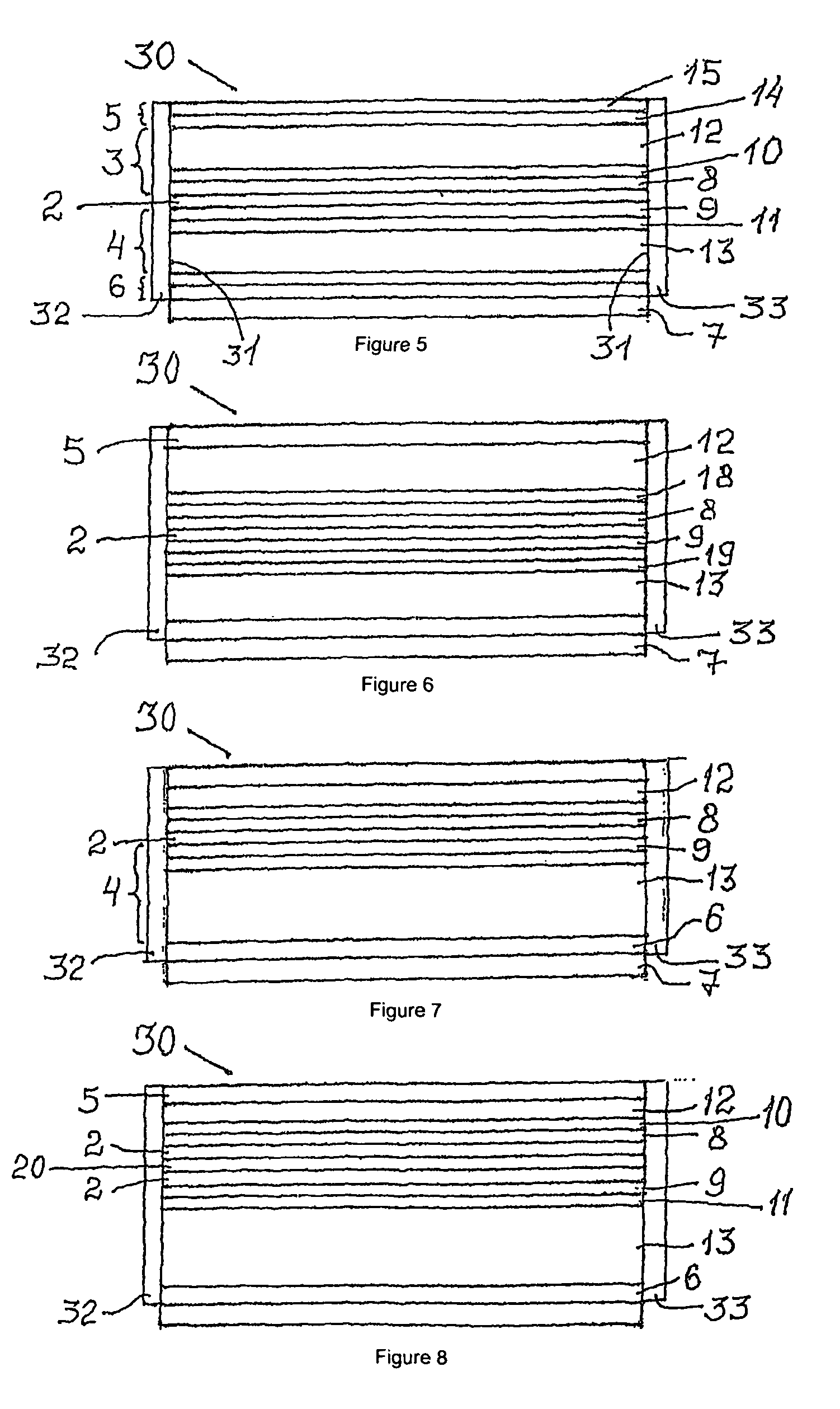
[0107]The proposed heterostructure 1 (see FIG. 1) contains one active layer 2, on each side of which two leak-in regions 3 and 4 were adjacent. To the leak-in regions 3 and 4 on each external (relative to the active layer 2) side two reflective layers 5 and 6 were adjacent. The reflective layer 6 is located on the side of the substrate 7 of the n-type GaAs. The leak-in regions 3 and 4 each contains one main adjusting layer 8 and 9 adjacent to the active layer 2 on each of its side, each one of confining layers 10 and 11 adjacent respectively to the main adjusting layers 8 and 9, and each o...


PUM


Abstract

The heterostructures are used for creation of semiconductor injection emission sources: injection lasers, semiconductor amplifying elements, semiconductor optical amplifiers that are used in fiber optic communication and data transmission systems, in optical superhigh-speed computing and switching systems, in development of medical equipment, laser industrial equipment, frequency-doubled lasers, and for pumping solid-state and fiber lasers and amplifiers. The heterostructure, the injection laser, the semiconductor amplifying element, and the semiconductor optical amplifier are proposed, the essential distinction of which consists in modernization of the active region and the leak-in region of the heterostructure, combined choice of location, compositions, refractive indices and thicknesses of the heterostructure layers providing the efficient functioning of the injection lasers, the semiconductor amplifying elements and the semiconductor optical amplifiers in the transient region of formation of controllable emission leak from the active layer.

Description

FIELD OF THE INVENTION[0001]The present invention relates to the key components of quantum electronic engineering, namely—to a heterostructure based on semiconductor compounds, an injection laser, a semiconductor amplifying element, and a semiconductor optical amplifier.DESCRIPTION OF THE RELATED ART[0002]Heterostructures are the base element for manufacturing of the efficient, high-power and compact semiconductor injection emission sources (hereinafter referred to as “IES”) with a narrow far-field pattern.[0003]Heterostructures for a semiconductor IES with leaky emission of a narrow far-field pattern are known [U.S. Pat. No. 4,063,189, 1977, H01S 3 / 19 331 / 94.5], [Patent 2142665 RU, 10.08.1998, H01S 3 / 19].[0004]From the standpoint of the technical result being solved an exemplary heterostructure is proposed in [Patent 2197049 RU, V. I. Shveikin, Russia, 18.02.2002, H01S 5 / 32]. The said prototype of heterostructure is based on semiconductor compounds and contains at least one active ...

Claims


Application Information

Patent Timeline
Patent Type & Authority Patents(United States)
IPC IPC(8): H01S5/00
CPCH01S5/4006H01S5/50H01S5/02284H01S5/028H01S5/2027H01S5/305H01S5/3054H01S5/3211H01S5/3213H01S5/323H01S5/02251H01S5/34H01S5/32
Inventor SHVEYKIN, VASILY IVANOVICH
Owner GENERAL NANO OPTICS
Why Eureka
Try Eureka