Electron beam exposure mask, electron beam exposure method, and electron beam exposure system

an electron beam and exposure method technology, applied in the field of electron beam exposure systems, can solve the problems of inability to equalize an energy in a pattern existing in a portion, inability to perform correction, and inability to planarize energy levels, etc., to achieve efficient correction of proximity effects, energy level can be planarized, and the rate of opening portion change can be changed.

Active Publication Date: 2010-12-07
ADVANTEST CORP
View PDF5 Cites 0 Cited by
  • Summary
  • Abstract
  • Description
  • Claims
  • Application Information

AI Technical Summary

Benefits of technology

[0015]The present invention has been accomplished in order to solve the above-described problems. An object of the present invention is to provide an auxiliary exposure mask necessary for precisely correcting a proximity effect occurring in a peripheral portion of a device formation pattern using cell projection method, to provide a method of correcting a proximity effect using the mask, and to provide an electron beam exposure system which corrects a proximity effect.
[0019]In the present invention, in order to planarize a portion in which an accumulated energy is inclined in a peripheral portion of a device formation pattern, an exposure is performed using an auxiliary exposure mask having opening portions arranged so that the sizes of the opening portions change at a predetermined rate in order of arrangement. Thus, a proximity effect occurring in the peripheral portion can be appropriately corrected by a cell projection method.
[0020]Further, the rate of the change of the opening portions can be changed by adjusting a light exposure. This makes it possible to cope with a change in energy by appropriately providing a light exposure for an auxiliary exposure mask even in the case where the slope of an accumulated energy varies depending on the shape of a pattern, eliminates the necessity for fabricating a mask for each energy slope, and makes it possible to efficiently correct a proximity effect.
[0021]Furthermore, by performing an auxiliary exposure out of focus, a pattern configured for an auxiliary exposure is not resolved, and an energy level can be planarized. Thus, a desired pattern can be more precisely exposed to light.

Problems solved by technology

In this case, since variable-shaped exposure is used, the patterns are individually exposed to light, and an enormous amount of time is needed compared to that for cell projection method.
Accordingly, if there is no space for that, correction cannot be performed.
Additionally, though an auxiliary light exposure is determined depending on the device formation pattern, it is difficult to equalize an energy in a pattern existing in a portion in which an accumulated energy is inclined in a peripheral portion with an energy equivalent to that in an inner portion.

Method used


Image

  • Electron beam exposure mask, electron beam exposure method, and electron beam exposure system
  • Electron beam exposure mask, electron beam exposure method, and electron beam exposure system
  • Electron beam exposure mask, electron beam exposure method, and electron beam exposure system

Examples


first embodiment

Constitution of Electron Beam Exposure System

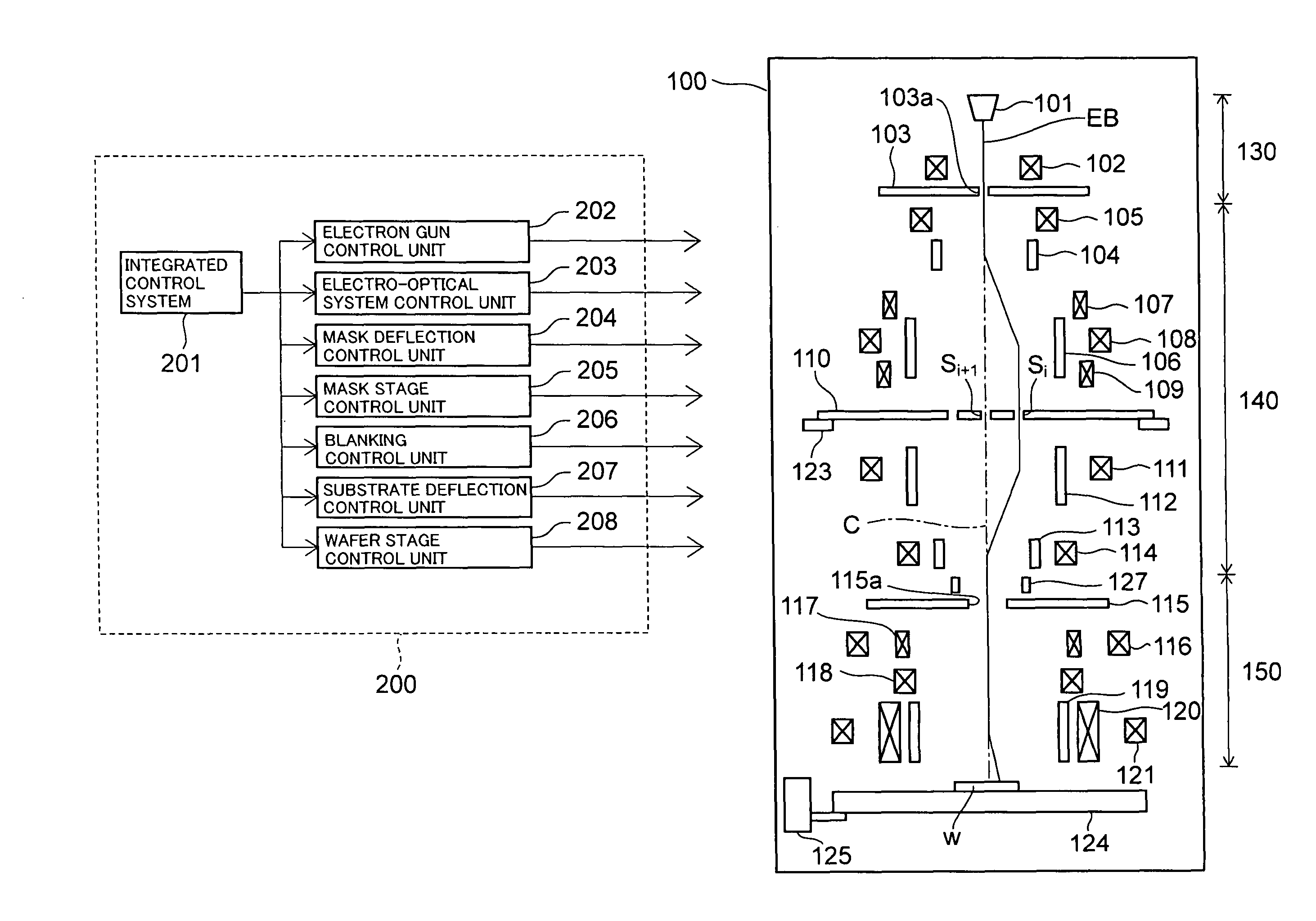
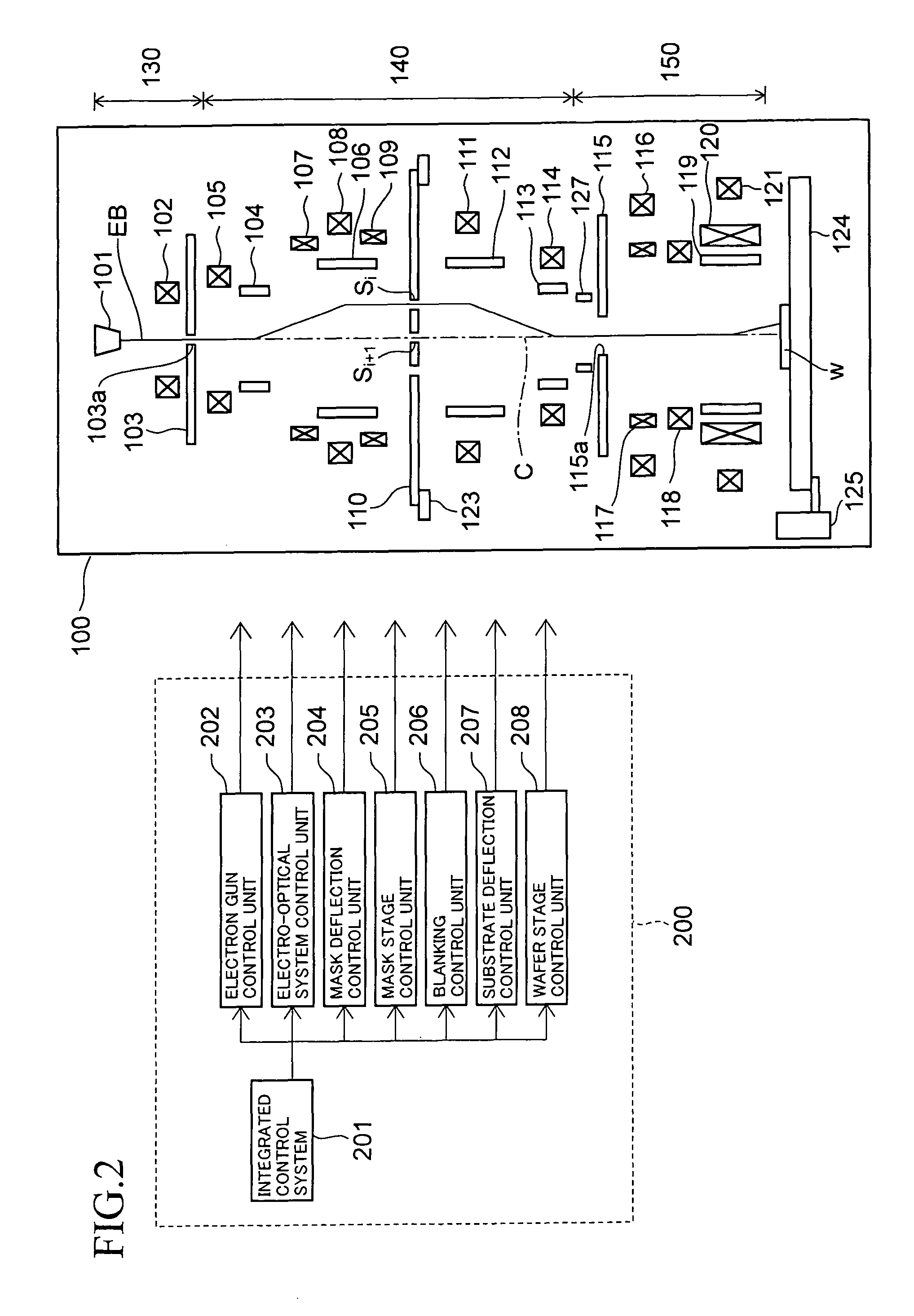
[0038]FIG. 2 is a diagram of the constitution of an electron beam exposure system according to this embodiment.

[0039]This electron beam exposure system is broadly divided into an electro-optical system column 100 and a control unit 200 which controls each unit of the electro-optical system column 100. The electro-optical system column 100 includes an electron beam generation unit 130, a mask deflection unit 140, and a substrate deflection unit 150, and the inside of the electro-optical system column 100 is decompressed.

[0040]In the electron beam generation unit 130, an electron beam EB generated in an electron gun 101 is converged in a first electromagnetic lens 102, and then passes through a rectangular aperture 103a of a beam-shaping mask 103, whereby the cross section of the electron beam EB is shaped into a rectangular shape.

[0041]After that, an image of the electron beam EB is formed onto an exposure mask 110 by a second electromagne...

second embodiment

[0072]With respect to the first embodiment, a description has been made for the case where an accumulated energy distribution in a peripheral portion of a device formation pattern is inclined linearly in the X direction. With respect to the second embodiment, a description will be made for the case where an accumulated energy distribution in a peripheral portion of a device formation pattern is inclined in arbitrary directions.

[0073]FIG. 11 is a diagram schematically showing slope directions of an accumulated energy distribution in a peripheral portion of a device formation pattern.

[0074]As shown in FIG. 11, in the case where a region in which a pattern is written is rectangular, the energy distribution in a peripheral portion is affected not only by the accumulated energy in the X direction but also by the accumulated energy in the Y direction as well. Accordingly, the slope of the energy distribution is shifted toward the Y direction. For example, in the case where the writing reg...

third embodiment

[0079]In the first embodiment, the case where an accumulated energy distribution in a peripheral portion decreases linearly has been described. However, there may be cases where energy decreases quadratically, depending on the shape of a pattern, the type of resist, and the like. In such a case, a proximity effect can be corrected by preparing and using an auxiliary exposure mask, such as the mask shown in FIG. 15, which changes from a large opening 49a to a small opening 49b so that a light exposure changes quadratically. Further, the energy distribution can also be planarized by sectioning a slope region of the energy distribution into small pieces and using the auxiliary exposure mask used in the first embodiment. After the slope portion has been planarized by any of these methods, an exposure is performed by adjusting the light exposure for a device formation pattern as in the first embodiment, whereby a desired pattern can be obtained.


PUM

PropertyMeasurementUnit
side lengthsaaaaaaaaaa
sizeaaaaaaaaaa
sizeaaaaaaaaaa

Abstract

An electron beam exposure system is designed to correct a proximity effect. The electron beam exposure system includes: an electron beam generation unit for generating an electron beam; an electron beam exposure mask having opening portions that are arranged so that sizes of the opening portions change at a predetermined rate in order of arrangement; a mask deflection unit for deflecting the electron beam on the electron beam exposure mask; a substrate deflection unit for deflecting and projecting the electron beam onto a substrate; and a control unit for controlling deflection amounts in the mask deflection unit and the substrate deflection unit. The direction or directions of the change may be any one of a row direction and a column direction or may be the row and column directions.

Description

CROSS-REFERENCE TO RELATED APPLICATIONS[0001]This application is based on and claims priority of Japanese Patent Application No. 2004-281321, filed on Sep. 28, 2004, the entire contents of which are being incorporated herein by reference.BACKGROUND OF THE INVENTION[0002]1. Field of the Invention[0003]The present invention relates to an electron beam exposure mask, an electron beam exposure method, and an electron beam exposure system, which correct a proximity effect in an electron beam exposure.[0004]2. Description of the Prior Art[0005]In recent years, electron beam exposure systems have come to be used in order to form fine patterns in lithography processes in the manufacture of semiconductor devices and the like.[0006]It is known that, in an electron beam exposure system, there occurs a phenomenon in which line widths and the like of a pattern transferred onto resist deviate from the designed values because of influences of a so-called proximity effect in which incident electron...

Claims


Application Information

Patent Timeline
Patent Type & Authority Patents(United States)
IPC IPC(8): A61N5/00G03F1/20G03F7/20H01J37/305H01L21/027
CPCB82Y10/00B82Y40/00G03F1/20H01J37/3174H01J2237/31769
Inventor YASUDA, HIROSHIYAMADA, AKIO
Owner ADVANTEST CORP
Why Eureka
Try Eureka