
Single-walled carbon nanotube and aligned single-walled carbon nanotube bulk structure, and their production process, production apparatus and application use

a single-walled carbon nanotube, carbon nanotube technology, applied in the direction of nanostructure manufacture, energy-based chemical/physical/physico-chemical processes, nanotubes, etc., can solve the problems of increasing the growth rate, not being able to achieve the patterning of single-walled carbon nanotubes, and prolonging the catalyst activity. the effect of the catalyst activity

Active Publication Date: 2010-12-21
NAT INST OF ADVANCED IND SCI & TECH
View PDF5 Cites 84 Cited by
  • Summary
  • Abstract
  • Description
  • Claims
  • Application Information

AI Technical Summary

Benefits of technology

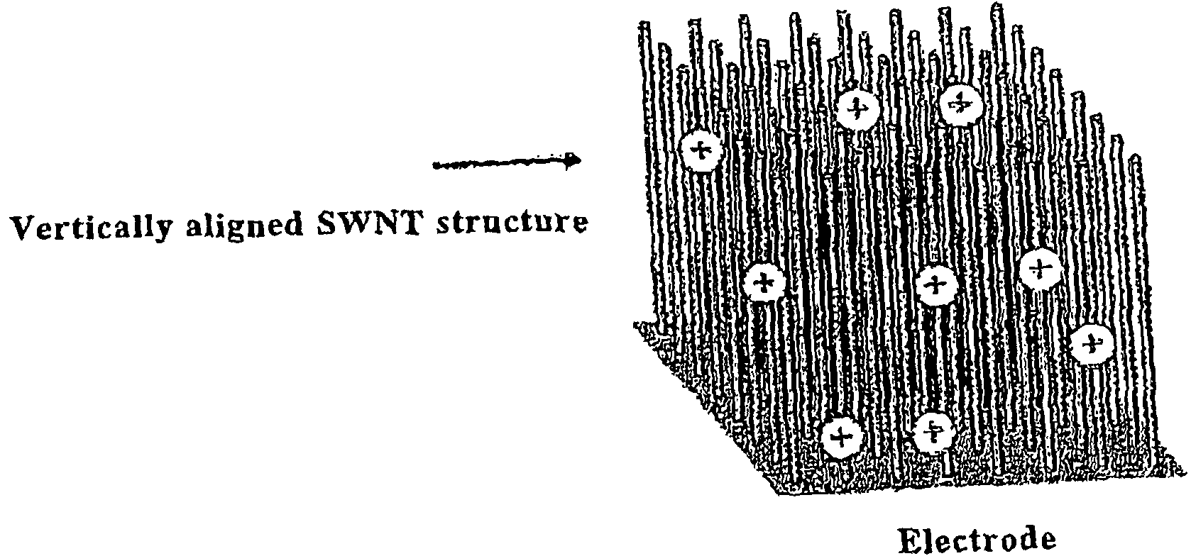
The present invention provides a method for producing high-purity, high-specific surface area, and aligned single-walled carbon nanotubes in large quantities without the use of special organic materials. This method allows for efficient growth and patterning of carbon nanotubes, as well as the use of a simple and convenient production process. The resulting carbon nanotubes have excellent purity and specific surface area, and can be used in a variety of applications such as nano-electronic devices, nano-optical devices, and energy storage. The method also allows for the growth of carbon nanotubes on a substrate, which further expands their potential applications.

Problems solved by technology

However, with all such a proposal, extension of the lifetime of the catalyst activity and increase in the growth rate have not yet been satisfactory also with a practical point of view at present.
However, while patterning has been attained in some multi-walled carbon nanotubes (Science 283, 412 (1999)), attainment of patterning for the single-walled carbon nanotubes has not yet been reported.
However, the single-walled carbon nanotubes tend to be adhered intensely to each other because of a strong Van der Waals force and constitute a disordered and non-aligned bulk structure, for example, during purification for removing impurities and re-construction of once formed not-order and not-alignment bulk structure is extremely difficult, for example, due to the difficulty in dispersing the single-walled carbon nanotubes in a solution and, with the reasons, such a bulk structure has not yet been obtained at present.

Method used


Image

  • Single-walled carbon nanotube and aligned single-walled carbon nanotube bulk structure, and their production process, production apparatus and application use
  • Single-walled carbon nanotube and aligned single-walled carbon nanotube bulk structure, and their production process, production apparatus and application use
  • Single-walled carbon nanotube and aligned single-walled carbon nanotube bulk structure, and their production process, production apparatus and application use

Examples


example 1

[0299]A carbon nanotube was grown by CVD method under the following conditions.

[0300]Carbon compound: ethylene; feed rate at 50 sccm

[0301]Atmosphere (gas) (Pa): helium, hydrogen gas mixture; feed rate at 1,000 sccm[0302]Pressure: 1 atm

[0303]water vapor addition amount (ppm): 300 ppm

[0304]Reaction temperature (° C.): 750° C.

[0305]Reaction time (min): 10 min

[0306]Metal catalyst (existent amount): iron thin film; 1 nm thickness

[0307]Substrate: silicon wafer

[0308]The catalyst was disposed on a substrate by using a sputtering vapor deposition apparatus and vapor depositing an iron metal to a thickness of 1 nm.

[0309]A relation between the reaction time and the growth state of the vertically aligned single-walled carbon nanotube (height), under the conditions described above was examined. The result is shown in FIG. 24.

[0310]Further, for the comparison, the growth state of the vertically aligned single-walled carbon nanotube was examined (existent CVD method) in the same manner as describe...

example 2

[0312]A carbon nanotube was grown by CVD method under the following conditions.

[0313]Carbon compound: ethylene; feed rate at 100 sccm

[0314]Atmosphere (gas): helium, hydrogen gas mixture; feed rate at 1,000 sccm[0315]Pressure: 1 atm

[0316]Water vapor addition amount (ppm): 175 ppm

[0317]Reaction temperature (° C.): 750° C.

[0318]Reaction time (min): 10 min

[0319]Metal catalyst (existent amount): iron thin film; 1 nm thickness

[0320]Substrate: silicon wafer

[0321]The catalyst was disposed on a substrate by using a sputtering vapor deposition apparatus and vapor depositing an iron metal to a thickness of 1 nm.

[0322]FIG. 26 shoes images formed by printing photographs, taken-up by a digital camera, of vertically aligned single-walled carbon nanotubes grown under the conditions described above. FIG. 26 shows the vertically aligned single-walled carbon nanotubes grown to a height of about 2.5 mm at the center, a match stick on the left, and a ruler with one gradation for 1 mm on the right.

[0323]...

example 3

[0328]A carbon nanotube was grown by CVD method under the following conditions.

[0329]Carbon compound: ethylene; feed rate at 75 sccm

[0330]Atmosphere (gas): helium, hydrogen gas mixture; feed rate at 1,000 sccm[0331]Pressure: 1 atm

[0332]Water vapor addition amount (ppm): 400 ppm

[0333]Reaction temperature (° C.): 750° C.

[0334]Reaction time (min): 10 min

[0335]Metal catalyst (existent amount): iron thin film; 1 nm thickness

[0336]Substrate: silicon wafer

[0337]The catalyst was disposed on a substrate by using a sputter vapor deposition apparatus and vapor depositing an iron metal to a thickness of 1 nm.

[0338]The peeling property of the vertically aligned single-walled carbon nanotubes produced as described above was examined. Peeling was conducted by using tweezers.

[0339]FIG. 33 shows a state of vertically aligned single-walled carbon nanotubes before peeling taken-up by a digital camera, FIG. 34 shows a state after peeling and FIG. 35 shows as-grown single-walled carbon nanotube purifica...


PUM

PropertyMeasurementUnit
specific surface areaaaaaaaaaaa
sizeaaaaaaaaaa
sizeaaaaaaaaaa

Abstract

This invention provides an aligned single-layer carbon nanotube bulk structure, which comprises an assembly of a plurality of aligned single-layer carbon nanotube and has a height of not less than 10 μm, and an aligned single-layer carbon nanotube bulk structure which comprises an assembly of a plurality of aligned single-layer carbon nanotubes and has been patterned in a predetermined form. This structure is produced by chemical vapor deposition (CVD) of carbon nanotubes in the presence of a metal catalyst in a reaction atmosphere with an oxidizing agent, preferably water, added thereto. An aligned single-layer carbon nanotube bulk structure, which has realized high purify and significantly large scaled length or height, its production process and apparatus, and its applied products are provided.

Description

[0001]This application is a U.S. national stage of International Application No. PCT / JP2005 / 014239 filed Jul. 27, 2005.TECHNICAL FIELD[0002]The present invention relates to a carbon nanotube (CNT) and an aligned single-walled carbon nanotube bulk structure, as well as their production process, production apparatus and application use and, more specifically, it relates to a carbon nanotube and an aligned single-walled carbon nanotube bulk structure attaining high purity, high specific surface area, large scale, and patterning, not found so far, and their production process, apparatus, and use.BACKGROUND ART[0003]For carbon nanotubes (CNT) for which development of functional materials has been expected as new electronic device materials, optical device materials, conductive materials, bio-related materials, etc., studies have been progressed earnestly for yield, quality, use, productivity, production process, etc.[0004]One of methods for producing carbon nanotubes includes a chemical ...

Claims


Application Information

Patent Timeline
Patent Type & Authority Patents(United States)
IPC IPC(8): B32B9/00D01F9/12B82Y10/00B82Y20/00B82Y30/00B82Y99/00C01B3/00C01B31/02G02B1/04H01B1/04H01L21/28H01L21/3205H01L21/768H01L23/532H01M4/587H01M4/86H01M4/96
CPCB82Y30/00B82Y40/00C01B31/026C01B2202/02C01B2202/08Y02E60/324C01B2202/34Y10S977/742Y10S977/75Y10T428/30Y10T428/2918C01B2202/30C01B32/162C01B32/17C01B32/178B82B1/008C01B32/18B82B3/0009Y02E60/32
Inventor HATA, KENJIIIJIMA, SUMIOYUMURA, MOTOOFUTABA, DON N.
Owner NAT INST OF ADVANCED IND SCI & TECH
Learn More