MEMS based RF components with vertical motion and parallel-plate structure and manufacture thereof using standard CMOS technologies

Inactive Publication Date: 2010-12-28
SIAMAK FOULADI AZARNAMINY +2
View PDF4 Cites 20 Cited by
  • Summary
  • Abstract
  • Description
  • Claims
  • Application Information

AI Technical Summary

Benefits of technology

[0011]The method further includes wet isotropic and anisotropic etching of the exposed sacrificial layer and the CMOS substrate for a controlled amount of time, respectively. The metal sacrificial layer is removed to form an air gap between the plates of the MEMS device. The removal of the silicon substrate is necessary to form a trench under the device and to improve its RF performance. The method also includes removing the etch resistant metal layer used as a mask during the first RIE stage of the CMOS dielectric layer.
[0013]In another embodiment, the method includes thinning of the dielectric layer present in the dielectric / metal and dielectric / metal / dielectric composite layers of the top and bottom plates of the microstructure, respectively. The controlled wet etching of the dielectric layer allows adjusting the air gap between the plates and also results in lowering the mechanical stiffness of the plates reducing the actuation voltage of the MEMS device.
[0015]It is a further object of the present invention to provide a MEMS variable capacitor built in CMOS technology. According to one embodiment, the MEMS variable capacitor includes a first curled-plate including a first composite metal / dielectric layer and a first underlying bottom plate having a composite dielectric / metal / dielectric layer. The plates of the disclosed RF-MEMS variable capacitor are intentionally curled upward to control the tuning performance of the device.
[0017]It is a further object of the present invention to provide integrated RF-MEMS tunable matching networks. According to one embodiment, the matching network includes a coplanar waveguide (CPW) transmission line periodically loaded with parallel-plate capacitive MEMS bridges between the signal and ground lines. Both the effective electrical length and characteristic impedance of the line is adjusted by employing the variable loading effect of the MEMS bridges. In another embodiment, the tunable matching circuit consists of a lumped-element network comprising of an integrated micromachined inductor with a high quality factor and an RF-MEMS parallel-plate variable capacitor. The disclosed matching circuit enables the implementation of CMOS reconfigurable amplifiers operating with their maximum efficiency under variable source / load impedance conditions.
[0024]An integrated intelligent adaptive system comprises RF MEMS structures having a compact size and low power consumption with improved RF performance, the system being integrated in a chip.

Problems solved by technology

However, with radio frequency (RF) passive components, as the transmitter chip size becomes smaller and smaller, RF passives remain a bottleneck for system miniaturization.

Method used


Image

  • MEMS based RF components with vertical motion and parallel-plate structure and manufacture thereof using standard CMOS technologies
  • MEMS based RF components with vertical motion and parallel-plate structure and manufacture thereof using standard CMOS technologies
  • MEMS based RF components with vertical motion and parallel-plate structure and manufacture thereof using standard CMOS technologies

Examples


Embodiment Construction

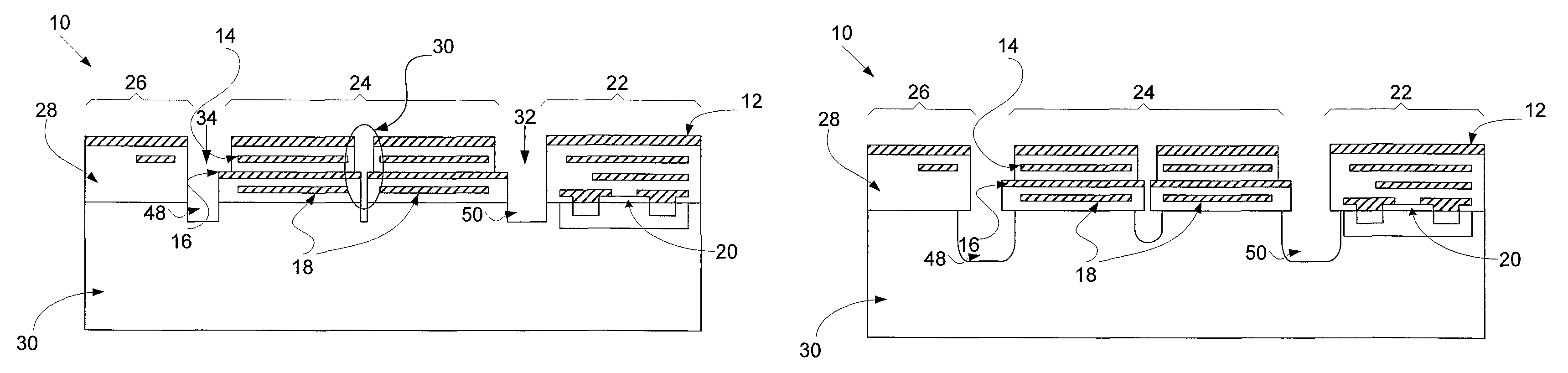
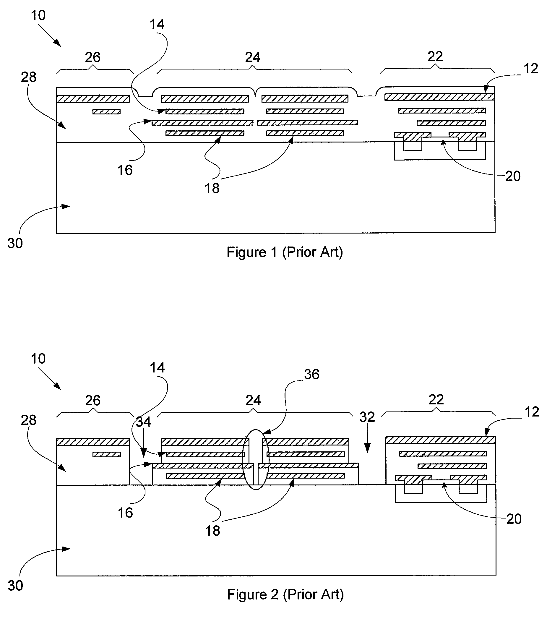
[0051]FIGS. 1 to 4 illustrate various post-processing stages used to implement the parallel-plate microstructure with vertical motion 10 according to one embodiment of the present invention. FIG. 1 shows the die after the standard CMOS processing. This could be any standard CMOS technology with at least four interconnect metal layers 12, 14, 16, and 18 and poly silicon layers 20. The CMOS die may include CMOS active circuitries 22, MEMS structures 24 and interconnect regions 26 formed using the conventional CMOS processing on a substrate material 30 such as silicon, for example. The metal layers 12, 14, 16 and 18 may comprise aluminium (Al) or copper (Cu). The dielectric material 28 between these metal layers could be any oxide material such as silicon dioxide.

[0052]FIG. 2 shows the microstructure 10 after anisotropic RIE removal of portions of the CMOS dielectric layer 28 according to the prior art. Readers may refer to U.S. Pat. No. 6,458,615 to Fedder et al., which is incorporate...


PUM


Abstract

A process of manufacturing parallel-plate microstructures by integrating the microstructures in a chip using a CMOS process is provided. A MEMS variable capacitor, a tunable band-pass filter, tunable matching networks, and capacitive RF-MEME switches all having vertically movable components and are integrated into a chip.

Description

BACKGROUND OF THE INVENTION[0001]1. Field of the Invention[0002]This invention relates to MEMS based RF components and a method of fabrication thereof, using CMOS technologies. The components are parallel-plate microstructures with vertical motion and include variable capacitors, filters, adaptive matching networks, reconfigurable amplifiers and switches. A process of manufacturing the CMOS-MEMS RF devices uses a dry reactive-ion etching process and a wet etching process.[0003]2. Detailed Description of the Prior Art[0004]It is known to have electronic systems in which all of the components are integrated into a single small-size wafer and packaged as a chip. It is known in active semi-conductor process technology to have all of the components integrated into a single chip. However, with radio frequency (RF) passive components, as the transmitter chip size becomes smaller and smaller, RF passives remain a bottleneck for system miniaturization.[0005]The advances of microelectronics m...

Claims


Application Information

Patent Timeline
Patent Type & Authority Patents(United States)
IPC IPC(8): H01L21/00
CPCB81C1/00246H01G5/16H01L28/40B81B2201/0271B81B2203/053B81C2203/0714B81C2203/0735
Inventor SIAMAK, FOULADI AZARNAMINYBAKRI-KASSEM, MAHERRAAFAT R., MANSOUR
Owner SIAMAK FOULADI AZARNAMINY
Why Eureka
Try Eureka