Interfacial layers for electromigration resistance improvement in damascene interconnects

a damascene interconnect and interfacial layer technology, applied in the direction of resistive material coating, semiconductor/solid-state device details, superimposed coating process, etc., can solve the problems of void formation within the interconnect, failure of the device, and failure of the electromigration resistance, so as to improve the electromigration resistance and the effect of greater adhesion

Active Publication Date: 2010-12-28
NOVELLUS SYSTEMS
View PDF32 Cites 47 Cited by
  • Summary
  • Abstract
  • Description
  • Claims
  • Application Information

AI Technical Summary

Benefits of technology

[0024]The devices formed using these methods may have improved electromigration proper

Problems solved by technology

One challenging problem encountered during IC fabrication is electromigration failure.
Electromigration occurs when high current densities experienced by an interconnect lead to migration of metal atoms with the current, and, consequently, lead to formation of voids within interconnects.
Ultimately, formation of voids may lead to failure of the device, known as electromigration failure.
As a consequence, the probability of electromigration failure increases with such device miniaturization.
While co

Method used


Image

  • Interfacial layers for electromigration resistance improvement in damascene interconnects
  • Interfacial layers for electromigration resistance improvement in damascene interconnects
  • Interfacial layers for electromigration resistance improvement in damascene interconnects

Examples


experimental example

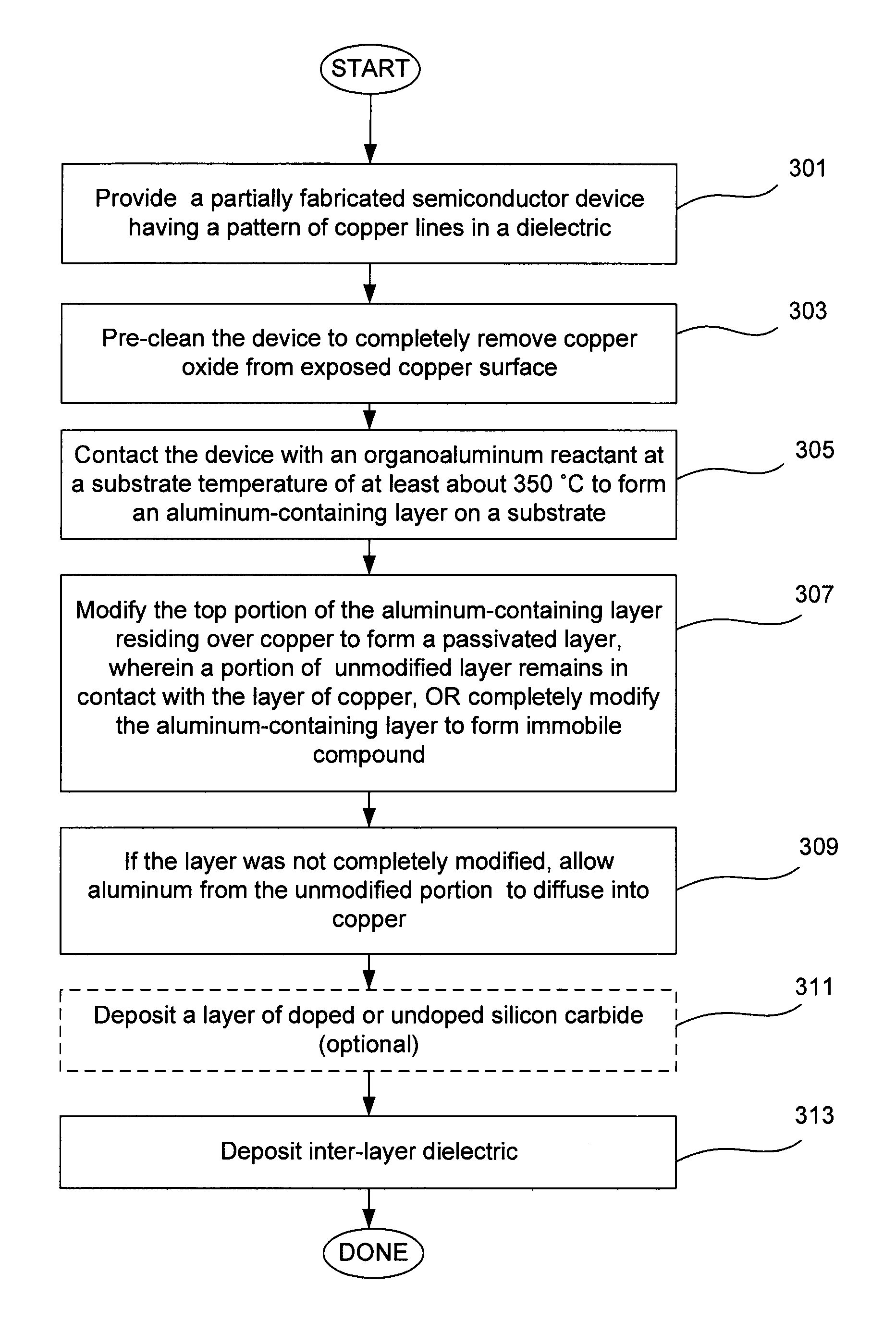
[0139]Fabrication of a copper interconnect having a boron-doped protective cap and a passivated layer containing boron and nitrogen will be illustrated with a reference to an experimental example.

[0140]In the described example, the process is started by a plasma pre-clean operation. The partially fabricated semiconductor device having an exposed pattern of copper lines in an ultra low-k dielectric (k=2.5; 5,000 Å thick) was obtained after a CMP operation, and was placed into a process chamber of a PECVD VECTOR™ apparatus. The entire capping process was performed at one station of a four-station apparatus. First, the substrate was pre-heated to 350° C., and H2 was introduced into the process chamber at a flow rate of 4,000 sccm. H2 was flown from second 0 to second 30 of the process time at a pressure of 4 Torr. At second 30 of the process time, HF RF plasma was ignited and was sustained at a power of 1.23 W / cm2 until second 45 of the process time. After the substrate was pre-cleaned...


PUM

PropertyMeasurementUnit
Temperatureaaaaaaaaaa
Electrical resistanceaaaaaaaaaa

Abstract

Protective caps residing at an interface between metal lines and dielectric diffusion barrier (or etch stop) layers are used to improve electromigration performance of interconnects. Protective caps are formed by depositing a first layer of aluminum-containing material over an exposed copper line by treating an oxide-free copper surface with an organoaluminum compound in an absence of plasma at a substrate temperature of at least about 350° C. The formed aluminum-containing layer is passivated either partially or completely in a chemical conversion which forms Al—N, Al—O or both Al—O and Al—N bonds in the layer. Passivation is performed in some embodiments by contacting the substrate having an exposed first layer with an oxygen-containing reactant and/or nitrogen-containing reactant in the absence of plasma. Protective caps can be formed on substrates comprising exposed ULK dielectric. The aluminum-containing layer residing on the dielectric portion will typically spontaneously form non-conductive layer comprising Al—O bonds.

Description

CROSS REFERENCE TO RELATED PATENT APPLICATIONS[0001]This application claims priority under 35 USC 119(e) from U.S. Provisional Patent Application No. 61 / 183,924 naming Yu et al. as inventors, titled “Interfacial Capping Layers for Interconnects,” filed Jun. 3, 2009, which is incorporated herein by reference in its entirety for all purposes. This application is also a continuation-in-part of application Ser. No. 12 / 074,108 filed Feb. 28, 2008, titled “Interfacial layers for electromigration resistance improvement in damascene interconnects” (U.S. Pat. No. 7,648,899, issued on Jan. 19, 2010) by Ananda Banerji et al., which is incorporated herein by reference in its entirety and for all purposes.FIELD OF THE INVENTION[0002]The present invention pertains to methods of forming layers of material on a partially fabricated integrated circuit. Specifically, the invention pertains to methods for forming protective caps within copper lines for improving electromigration properties of Damascen...

Claims


Application Information

Patent Timeline
IPC IPC(8): H01L21/44B05D5/12
CPCC23C16/0227C23C16/0272C23C16/36H01L21/02074H01L21/76832H01L21/76834H01L21/76849H01L21/76867H01L21/76883H01L21/76886H01L21/76888H01L23/53238H01L23/53295H01L2924/0002H01L2924/00
Inventor BANERJI, ANANDAANTONELLI, GEORGE ANDREWO'LOUGHLIN, JENNIFERSRIRAM, MANDYAMVAN SCHRAVENDIJK, BARTVARADARAJAN, SESHASAYEE
Owner NOVELLUS SYSTEMS
Why Eureka
Try Eureka