FET-based sensor for detecting ionic material, ionic material detecting device using the FET-based sensor, and method of detecting ionic material using the FET-based sensor

a fet-based sensor and ionic material technology, applied in lighting and heating apparatus, drying machines with progressive movements, instruments, etc., can solve the problems of low sensitivity of biosensors, inability to separate signals derived from target biomolecules from noise, and inability to use signal correction, etc., to achieve low concentration of ionic materials and high sensitivity

Active Publication Date: 2010-12-28
SAMSUNG ELECTRONICS CO LTD
View PDF11 Cites 149 Cited by
  • Summary
  • Abstract
  • Description
  • Claims
  • Application Information

AI Technical Summary

Benefits of technology

[0012]An exemplary embodiment provides a field effect transistor (“FET”)-based sensor that can detect a low concentration of ionic materials with high sensitivity.
[0013]An exemplary embodiment provides an ionic material detecting device that can detect a low concentration of ionic materials with high sensitivity.

Problems solved by technology

Conventional FET-based biosensors, however, cannot separate signals derived from target biomolecules from noise, such as a drift signals spontaneously generated due to a reaction on a surface of a gate electrode, and signals generated due to the pressure of inflowing solution.
However, since the two FETs of the biosensor use different surface materials, signals from the reference FET do not show drifting, which occurs in the sensing FET, and thus cannot be used for signal correction.
Thus, the sensitivity of the biosensor is still low.

Method used


Image

  • FET-based sensor for detecting ionic material, ionic material detecting device using the FET-based sensor, and method of detecting ionic material using the FET-based sensor
  • FET-based sensor for detecting ionic material, ionic material detecting device using the FET-based sensor, and method of detecting ionic material using the FET-based sensor
  • FET-based sensor for detecting ionic material, ionic material detecting device using the FET-based sensor, and method of detecting ionic material using the FET-based sensor

Examples


example 1

Manufacture of a FET-Based Sensor for Ionic Material Detection

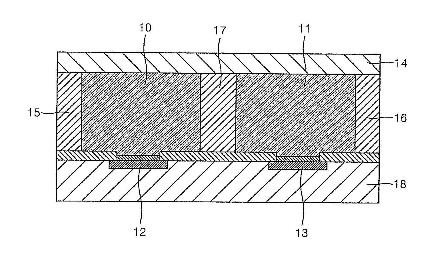
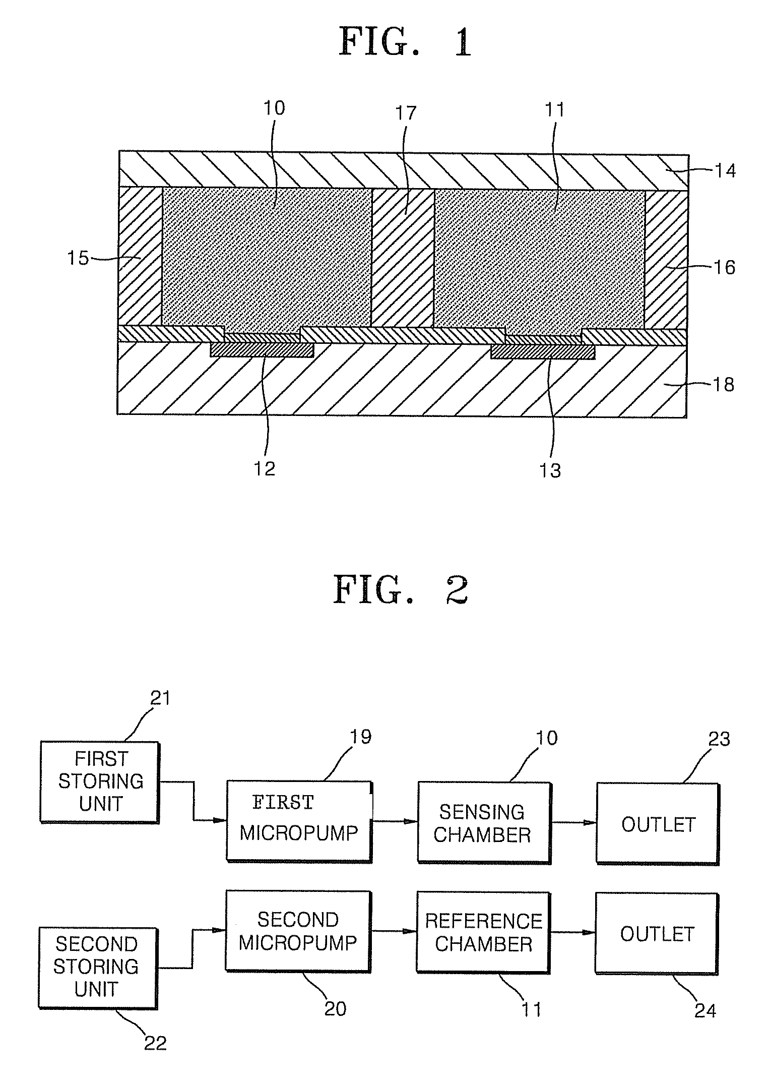
[0078]A FET device was order-manufactured by X-FAB Semiconductor Foundries (Germany). The manufactured FET device included 192 FETs having the same structure and the same electrical characteristics in an array of 4×48. The FET device was manufactured using the equipment of X-FAB Semiconductor Foundries according to the company's own CMOS process. Although companies may have different standard CMOS processes, such differences are not a substantial factor affecting characteristics of the FET device. Therefore, the CMOS standard process of the company is not described herein.

[0079]A passivation layer and a gate electrode layer were removed from each of the FETs in an array to expose a polysilicon layer. Next, the exposed polysilicon layer on the surface of the FET was carefully washed with pure acetone and then with water and dried. The process of washing the substrate was performed using a wet station used in semiconductor ...

experimental example 1

DNA Detection Using a FET-Based Sensor for Ionic Material Detection Including a Single Chamber

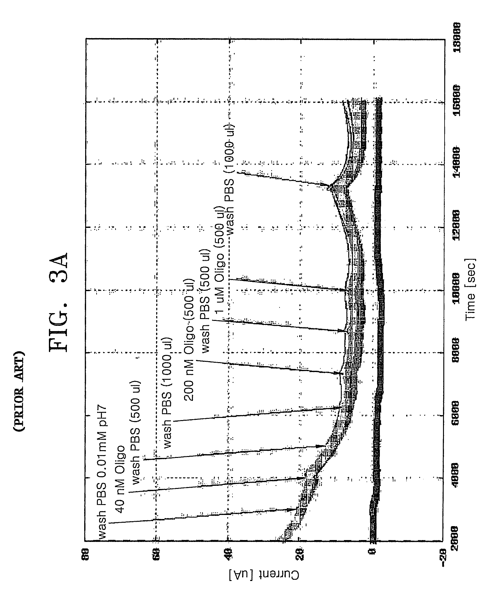
[0085]A 0.01 millimolar mM phosphate buffer solution (“PBS”) (e.g., pH 7.0) and a solution containing 15-mer oligonucleotide (TGTTCTCTTGTCTTG) (SEQ. ID. NO. 1) were alternately flowed into and out of a chamber of the FET-based sensor manufactured in Experimental Example 1.

[0086]In particular, a 0.01 mM PBS solution, a 40 nanomolar (nM) oligonucleotide solution, 500 microliter (μl) of a 0.01 Mm PBS solution, 1000 μl of PBS, 500 μl of 200 nM oligonucleotide solution, 500 μl of PBS, and 500 μl of a 1 micromolar (μM) oligonucleotide solution, and 1000 μl of PBS were sequentially flowed into the chamber at 0.5 microliter per minute (μl / min) with an interval of several minutes to allow a previously injected solution to be completely flowed out of the chamber while a next solution was injected.

[0087]The level of a current in each of the 24 FETs, including 12 sensing FETs and 12 reference FETs, of ...

experimental example 2

[0091]DNA Detection Using a FET Based Sensor (First Experiment)

[0092]A 0.01 mM PBS buffer solution (pH 7.0) was flowed into and out of each of the sensing chamber and the reference chamber of the FET-based sensor manufactured in Example 1 under the same pressure through each chamber. Next, at a certain point of time, the PBS buffer solution was flowed into and out of the reference chamber while a solution containing 15-mer oligonucleotide (TGTTCTCTTGTCTTG) (SEQ. ID. NO. 1) was flowed into and out of the sensing chamber under the same pressure as the PBS buffer solution was flowed into and out of the reference chamber.

[0093]In particular, the PBS solution was injected three times into each of the sensing chamber and the reference chamber, and at a certain point of time, the PBS solution was flowed into the reference chamber while the 1 μM oilgonucleotide solution was flowed into the sensing chamber. Next, the PBS solution was flowed three times into each of the reference chamber and ...


PUM

PropertyMeasurementUnit
pHaaaaaaaaaa
currentsaaaaaaaaaa
levels of currentsaaaaaaaaaa

Abstract

Provided are a FET-based sensor for detecting an ionic material, an ionic material detecting device including the FET-based sensor, and a method of detecting an ionic material using the FET-based sensor. The FET-based sensor includes: a sensing chamber including a reference electrode and a plurality of sensing FETs; and a reference chamber including a reference electrode and a plurality of reference FETs. The method includes: flowing a first solution into and out of the sensing chamber and the reference chamber of the FET-based sensor; flowing a second solution expected to contain an ionic material into and out of the sensing chamber while continuously flowing the first solution into and out of the reference chamber; measuring a current in a channel region between the source and drain of each of the sensing and reference FETs; and correcting the current of the sensing FETs.

Description

[0001]This application claims priority to Korean Patent Application No. 10-2006-0002373, filed on Jan. 9, 2006, and all the benefits accruing therefrom under 35 U.S.C. §119, the contents of which in its entirety are herein incorporated by reference.BACKGROUND OF THE INVENTION[0002]1. Field of the Invention[0003]The present invention relates to a FET-based sensor for detecting an ionic material, a device for detecting an ionic material including the FET-based sensor and a method of detecting an ionic material using the device.[0004]2. Description of the Related Art[0005]Transistor-based biosensors are a kind of sensors detecting ionic materials, especially biomolecules, using electrical signals in aqueous solution. Transistor-based biosensors are manufactured through semiconductor manufacturing processes and have been significantly researched due to the advantages of high-speed signal transition and easy combination with an integrated circuit (“IC”) and micro-electro mechanical syste...

Claims


Application Information

Patent Timeline
Patent Type & Authority Patents(United States)
IPC IPC(8): H01L29/78
CPCG01N33/54373G01N27/4145C12Q1/6825D06B13/00D06B15/09D06B23/023F26B5/02F26B13/00
Inventor LEE, KYU-SANGYOO, KYU-TAESHIM, JEO-YOUNGKIM, JIN-TAECHO, YEON-JA
Owner SAMSUNG ELECTRONICS CO LTD
Why Eureka
Try Eureka