Semiconductor integrated circuit and radio communication apparatus for communication

a radio communication apparatus and integrated circuit technology, applied in the direction of code conversion, phase-modulated carrier system, sustainable building, etc., can solve the problem of increasing chip cost, and achieve the effect of reducing the total power consumption of the radio communication apparatus

Inactive Publication Date: 2011-04-19
RENESAS ELECTRONICS CORP
View PDF22 Cites 11 Cited by
  • Summary
  • Abstract
  • Description
  • Claims
  • Application Information

AI Technical Summary

Benefits of technology

[0014]In view of the above problem, a technique has been proposed in which a high-frequency IC is provided with an A / D converter circuit and a D / A converter circuit and in which I and Q signals are transmitted as digital signals between the high-frequency IC and a baseband IC. In this arrangement, with the high-frequency IC being provided with an A / D converter circuit and a D / A converter circuit, the baseband IC requires no A / D converter circuit and no D / A converter circuit. This makes it unnecessary for the baseband IC production process to include a step for forming analog circuit elements, so that chip cost can be reduced. Also, when a baseband IC includes digital circuits only, it can be designed to be operable at a low supply voltage, for example, 1.8 V so as to reduce its power consumption. Furthermore, digitizing I and Q signals can improve the SN ratio (signal-to-noise ratio) of the circuit.
[0021]An object of the present invention is to reduce a total power consumption of a radio communication apparatus including a semiconductor integrated circuit for communication (high-frequency IC) and a baseband circuit, the semiconductor integrated circuit having functions for demodulating and downconverting a received signal and for modulating and upconverting a transmit signal.
[0022]Another object of the present invention is to obtain a desired frequency accuracy in a semiconductor integrated circuit for communication (high-frequency IC) incorporating an oscillator circuit which generates a reference clock signal for use in modulating a transmit signal and demodulating a received signal, even in a configuration where oscillation frequency information is given as a digital signal from a baseband circuit while avoiding increasing the circuit area.
[0026]When the above arrangement is used, the baseband circuit requires no A / D converter circuit and no D / A converter circuit. This makes it unnecessary for a baseband IC production process to include a step for forming analog circuit elements, so that chip cost can be reduced. Also, when a baseband IC includes digital circuits only, it can be designed to be operable at a low supply voltage, for example, 1.8 V so as to reduce its power consumption. This leads to a reduction in the total power consumption of a radio communication apparatus provided with a high-frequency IC and a baseband circuit.
[0028]According to the present invention, it is possible to reduce the total power consumption of a radio communication apparatus provided with a semiconductor integrated circuit for communication (high-frequency IC), which has functions for modulating / demodulating and upconverting / downconverting a transmit signal or a received signal, and a baseband circuit.

Problems solved by technology

This causes a problem of increasing chip costs.

Method used


Image

  • Semiconductor integrated circuit and radio communication apparatus for communication
  • Semiconductor integrated circuit and radio communication apparatus for communication
  • Semiconductor integrated circuit and radio communication apparatus for communication

Examples


Embodiment Construction

[0035]An embodiment of the present invention will be described in the following with reference to the accompanying drawings.

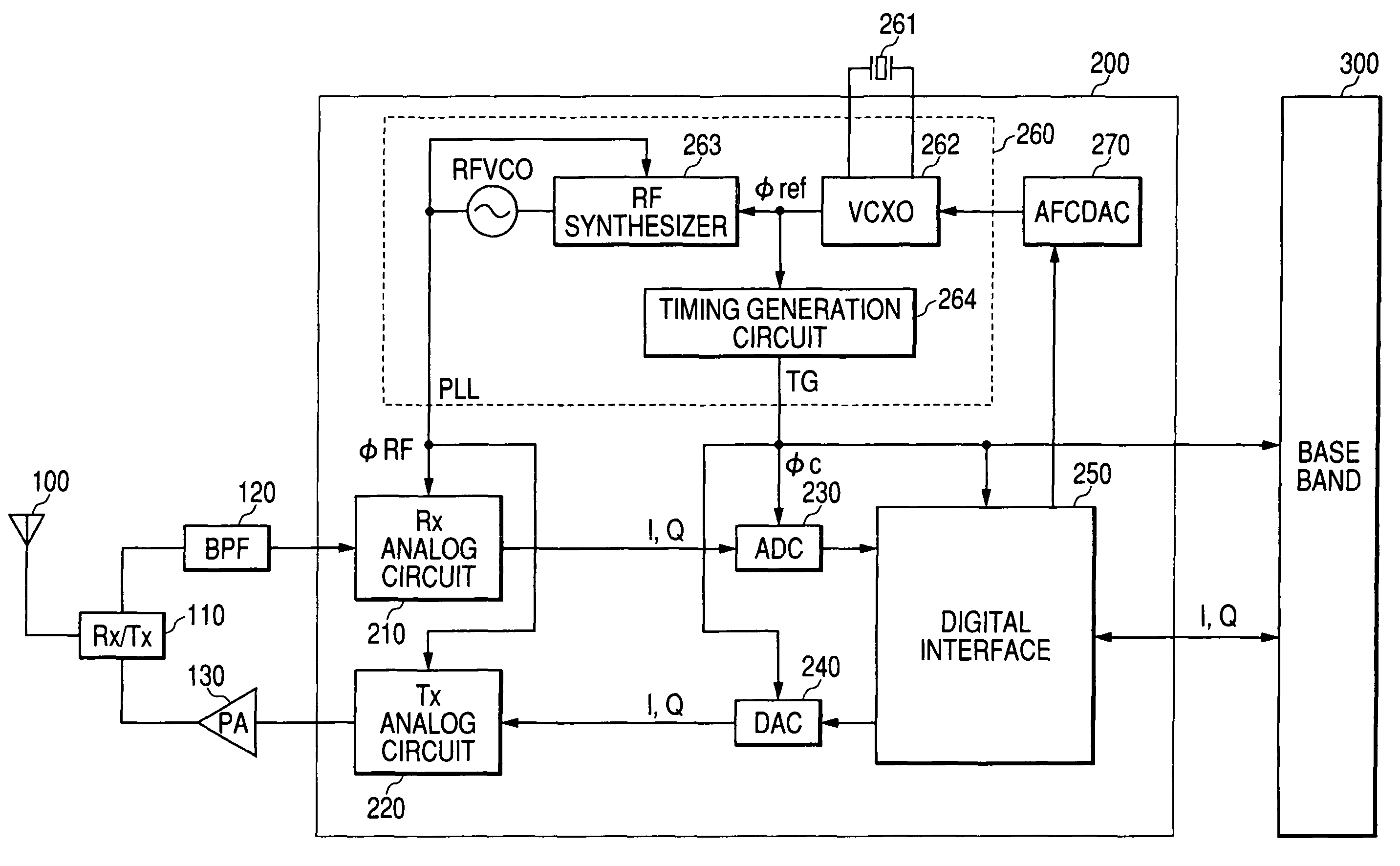
[0036]FIG. 1 shows an example of an overall configuration of a high-frequency IC and a radio communication apparatus according to the present invention, the IC and the apparatus being for GSM (including both narrowly-defined GSM in which GMSK modulation is made and broadly-defined GSM inclusive of EDGE mode in which 8PSK modulation is made) radio communication.

[0037]As shown in FIG. 1, the radio communication apparatus includes an antenna 100 for transmission and reception, a switch 110 for switching between transmission and reception, a band-pass filter 120 for removing unwanted waves from a received signal, a high-frequency power amplifier circuit 130, a high-frequency IC 200, and a baseband IC 300.

[0038]The high-frequency IC 200 has functions for demodulating and downconverting a received signal and for modulating and upconverting a transmit signal. The base...


PUM


Abstract

A total power consumption of a radio communication apparatus is reduced, the radio communication apparatus including a semiconductor integrated circuit (high-frequency IC) which has a clock generation circuit which generates a reference clock signal for use in modulating a transmit signal and demodulating a received signal. The clock generation circuit is provided with a voltage-controlled oscillator circuit (VCXO) which oscillates, when a quartz oscillator is connected thereto, at a frequency dependent on a natural frequency of the quartz oscillator and a control voltage applied thereto. The voltage-controlled oscillator circuit is configured such that a result obtained by converting, in an internal D / A converter circuit, digital frequency control information supplied from the baseband circuit is applied as the control voltage to the voltage-controlled oscillator circuit and such that the voltage-controlled oscillator circuit oscillates at a frequency corresponding to the control voltage.

Description

CROSS-REFERENCE TO RELATED APPLICATION[0001]The present application claims priority from Japanese patent application No. 2005-136986 filed on May 10, 2005, the content of which is hereby incorporated by reference into this application.BACKGROUND OF THE INVENTION[0002]The present invention relates to technology effective when applied to a semiconductor integrated circuit for communication incorporating a voltage-controlled oscillator circuit, particularly an oscillator circuit using a quartz oscillator, and a radio communication apparatus using the semiconductor integrated circuit for communication. The technology is effectively applicable, for example, in a high-frequency semiconductor integrated circuit incorporating an oscillator circuit which generates a reference clock signal for use in processing transmit and received signals, by being used in a case where oscillation frequency information as a digital signal is given from a baseband circuit.[0003]In the inventions described in...

Claims


Application Information

Patent Timeline
Patent Type & Authority Patents(United States)
IPC IPC(8): H04B1/38H04L27/00H04L7/00
CPCH03M1/0607H04L27/2272H03M1/682H03M1/765Y02B60/50H04L2027/0028H04L2027/0055
Inventor OKAZAKI, TAKAOFUKUCHI, SATORU
Owner RENESAS ELECTRONICS CORP
Why Eureka
Try Eureka