Method for forming a semiconductor film including a film forming gas and decomposing gas while emitting a laser sheet

a technology of laser sheet and film, applied in the direction of chemical vapor deposition coating, coating, electric discharge tube, etc., can solve the problems of film thickness on the substrate to vary in the direction, limit the production rate of thicker nc-si:h films by pecvd, and structural defects that have deleterious electrical properties

Active Publication Date: 2011-06-14
AUCMOS TECH USA INC
View PDF9 Cites 6 Cited by
  • Summary
  • Abstract
  • Description
  • Claims
  • Application Information

AI Technical Summary

Benefits of technology

Another object of the present invention is to provide a CVD apparatus which is capable of forming a dense semiconductor film under high-rate deposition conditions without damaging the same by simultaneously utilizing a laser sheet and a plasma to excite and decompose a film forming gas.
Still another object of present invention is to provide a CVD apparatus in which the laser transmission window remains substantially free of film product during film forming process on a substrate by a means for removing the film forming gas from the surface of the laser transmission window.
According to the present invention, the film forming gas in the chamber is excited and decomposed by the laser sheet, which passes in parallel with the substrate along a plane spaced apart therefrom, and concurrent ionization effected by the antenna, thereby forming a dense and uniform semiconductor film on the substrate at high rate. Moreover, during the film forming process on the substrate, the film forming gas in the reaction chamber is prevented from reaching the surface of the laser incidence window by flowing an inert gas through the purge port, to which the window is mounted.
According to the present invention, the film forming gas in the chamber is excited and decomposed by the laser sheet, which passes between the discharge electrode and the substrate in parallel with the substrate along a plane spaced apart therefrom, and concurrent ionization effected by the electrodes, thereby forming a dense and uniform semiconductor film on the substrate at high rate. The as-deposited film is then irradiated by the laser beam generated by the excimer laser, thereby changing the film crystallinity and increasing the film grain size.

Problems solved by technology

While a-Si:H based solar cells and TFT devices have been commercially produced by PECVD for years, the production of thicker nc-Si:H films by PECVD is limited by the deposition rate thereof.
As the film forming rate of nc-Si:H is increased by increasing the RF power input, however, the bombardment of the growing nc-Si:H film on the substrate by highly energized ions also increases, thereby generating film structural defects that have deleterious effects on electrical properties thereof.
However, there are several drawbacks in applying the conventional laser beam CVD process in production of solar cells and TFT devices, which requires dense and uniform semiconductor films deposited over large area substrates.
A problem associated with the conventional laser CVD process described above is that since the reaction product reaches the substrate surface by diffusing away from the laser effected zone, which is defined by the narrow path of the laser beam above the substrate, the concentration of the reaction product on the substrate surface will depend on the distance away from the path of the laser beam, thereby causing the film thickness on the substrate to vary in the direction perpendicular to the path of the laser beam.
While it is possible to improve the film uniformity on the substrate by increasing the distance between the beam path and the substrate surface, doing so will adversely decrease the film deposition rate.
Another problem associated with the conventional laser beam CVD process described above is that under high-rate deposition conditions, there is a propensity for the formation of nanoparticles from the gas phase reaction, thereby causing nanoparticles to directly deposit on the substrate surface (for instance, see U.S. Pat. No. 6,248,216 B1).
A film composed of aggregates of nanoparticles is inherently porous and has poor adhesion with the substrate compared with a monolithic film formed by condensation of reactant atoms or molecules on the substrate surface, such as films formed by the plasma CVD process.
Porosity in semiconductor films can cause oxidation, which would adversely affect the electrical properties thereof, and other reliability problems.
While bombardment of growing film by energetic ions may reduce film porosity, it will damage semiconductor films and have deleterious effects on electrical properties thereof as encountered in the PECVD process under high-rate deposition conditions.
Still another problem associated with the conventional laser CVD process described above is the clouding of the window surface inside the reaction chamber because film deposition occurs simultaneously on the surface of the window as the laser beam passes therethrough during the deposition on the substrate.
The laser-induced reactions and the film deposition process on the substrate eventually terminate as the reaction product on the window forms an opaque layer so thick that the laser beam cannot effectively pass therethrough.

Method used


Image

  • Method for forming a semiconductor film including a film forming gas and decomposing gas while emitting a laser sheet
  • Method for forming a semiconductor film including a film forming gas and decomposing gas while emitting a laser sheet
  • Method for forming a semiconductor film including a film forming gas and decomposing gas while emitting a laser sheet

Examples


first embodiment

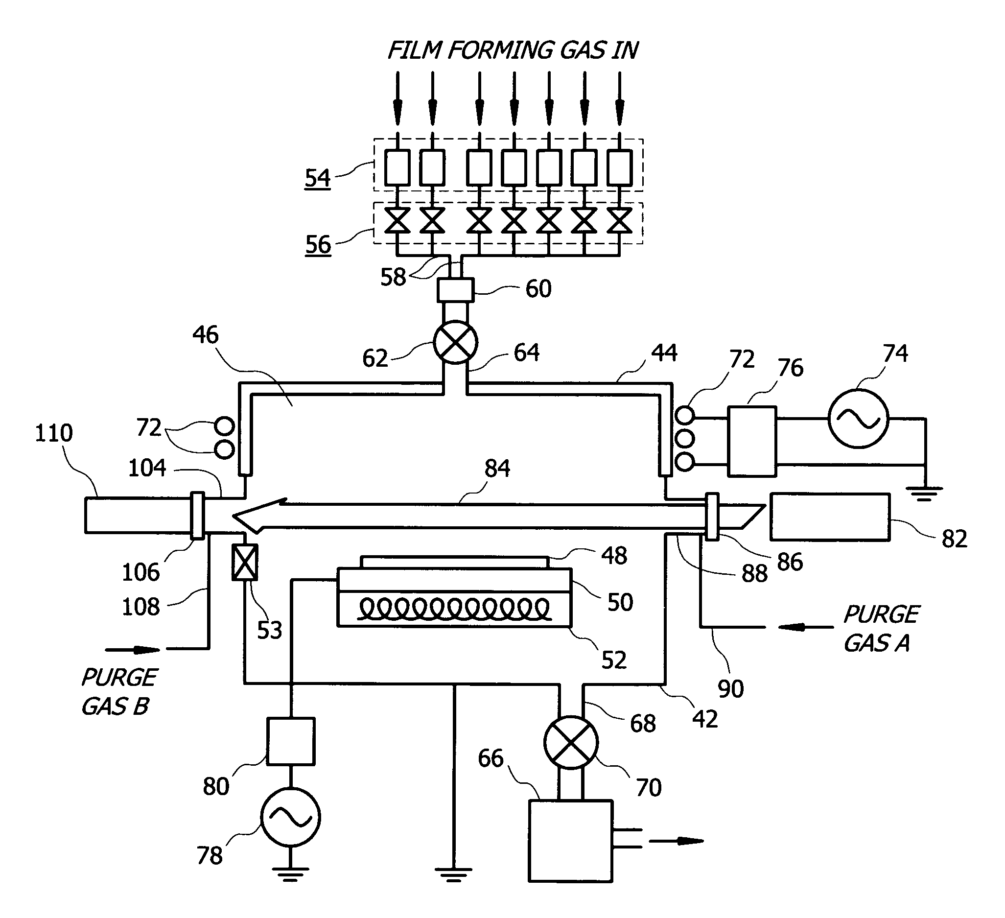
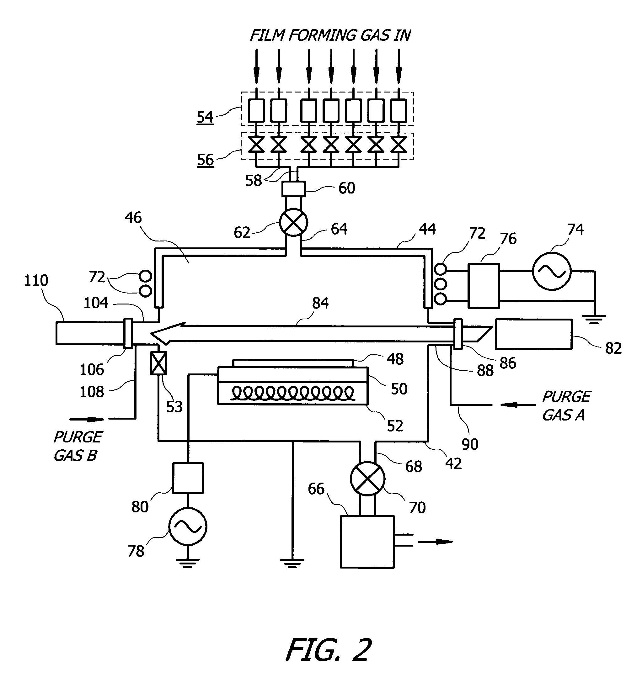
the present invention as applied to a high-rate chemical vapor deposition (CVD) apparatus for forming semiconductor thin films will now be described with reference to FIG. 2. Referring now to FIG. 2, the illustrated apparatus has a vessel base 42, preferably constructed of a suitably strong and conductive material such as stainless steel and is electrically grounded, and a vessel top or dome 44, which is made of a dielectric material such as aluminum oxide or aluminum nitride. The base 42 and the dome 44 combined to define a reaction chamber 46 therein.

A generally flat substrate 48 for coating a film thereon is placed inside the reaction chamber 46. The substrate 48 is supported by a mounting base 50, which also serves as a bias electrode. A suceptor 52 for heating the substrate 48 is attached to the bottom surface of the mounting base 50, and incorporates therein a heating element which may be energized from a current source (not shown) external to the chamber 46. The substrate 48 ...


PUM

PropertyMeasurementUnit
energyaaaaaaaaaa
thicknessaaaaaaaaaa
thicknessaaaaaaaaaa

Abstract

An apparatus for high-rate chemical vapor (CVD) deposition of semiconductor films comprises a reaction chamber for receiving therein a substrate and a film forming gas, a gas inlet for introducing the film forming gas into the reaction chamber, an incidence window in the reaction chamber for transmission of a laser sheet into the reaction chamber, a laser disposed outside the reaction chamber for generating the laser sheet and an antenna disposed outside the reaction chamber for generating a plasma therein. The film forming gas in the chamber is excited and decomposed by the laser sheet, which passes in parallel with the substrate along a plane spaced apart therefrom, and concurrent ionization effected by the antenna, thereby forming a dense semiconductor film on the substrate at high rate.

Description

BACKGROUND1. Field of InventionThe present invention relates to a method for depositing semiconductor films, and more particularly to a chemical vapor deposition (CVD) process utilizing plasma and laser excitation means for high-throughput manufacturing of solar cells devices.2. Description of Prior ArtHydrogenated amorphous silicon (a-Si:H) and nano-crystalline silicon (nc-Si:H) are widely used in thin film solar cells because they can be fabricated over large area substrates as required by photovoltaic applications. Compared with amorphous Si, nc-Si:H may produce solar cells with higher efficiency and is more stable against light induced degradation or the Staebler-Wronski effect. Because of its lower absorption coefficient in the visible range of the solar spectrum, however, the nc-Si:H layer in solar cells needs to be 1 to 3 um thick, which is 3 to 10 times thicker than that required of a-Si:H.Among various methods to form Si thin films over large area substrates, plasma-enhance...

Claims


Application Information

Patent Timeline
Patent Type & Authority Patents(United States)
IPC IPC(8): H01L21/20H01L21/36
CPCC23C16/22C23C16/24C23C16/325H01J37/32862C23C16/50C23C16/56H01J37/3244C23C16/483
Inventor CHEN, YUNG-TIN
Owner AUCMOS TECH USA INC
Why Eureka
Try Eureka