Organic electroluminescence device and organic laser diode

a laser diode and electroluminescence technology, applied in the direction of discharge tube/lamp details, organic semiconductor devices, discharge tubes luminescnet screens, etc., can solve the problems of optical propagation loss, damage or deterioration of organic films, and increase in the size of devices and others, and achieve narrow spectral width and low energy density.

Inactive Publication Date: 2011-06-21
KYUSHU UNIV
View PDF5 Cites 8 Cited by
  • Summary
  • Abstract
  • Description
  • Claims
  • Application Information

AI Technical Summary

Benefits of technology

The present invention has been developed for overcoming the above problems, and an object of the invention is to provide an organic EL device that can provide light having an extremely narrow spectral width even under excitation with a low energy density (current density).
The present invention provides the edge emitting type organic EL device that can emit the light having a narrow spectral width even under excitation of a low energy density (current density). According to the organic EL device of the present invention, the emitted light peak wavelength can be changed only by changing the film thickness of the light emitting layer so that a plurality of organic EL devices exhibiting the desired emitted light peak wavelength in an arbitrary visible range can be manufactured without difficulty.

Problems solved by technology

However, the optically pumped organic laser requires another light source for pumping a laser active material so as to obtain the laser beam, resulting in a problem of increase in size of a device and others.
However, this suffers from many problems such as (1) destruction or deterioration of an organic film due to heat generation with a large current density, (2) deactivation of excitons at a large current density due to interaction between excitons or interaction between excitons and polarons, (3) optical propagation loss due to light absorption by excitons, polarons and electrodes, and others.
However, these problems are not yet overcome sufficiently.

Method used


Image

  • Organic electroluminescence device and organic laser diode
  • Organic electroluminescence device and organic laser diode
  • Organic electroluminescence device and organic laser diode

Examples


example 1

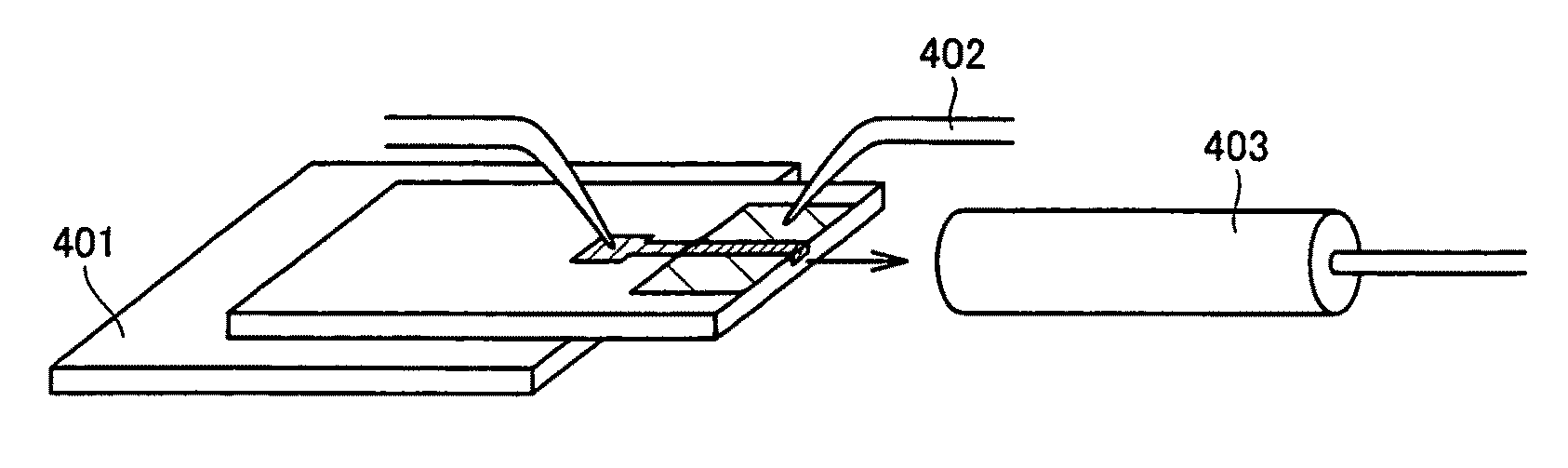
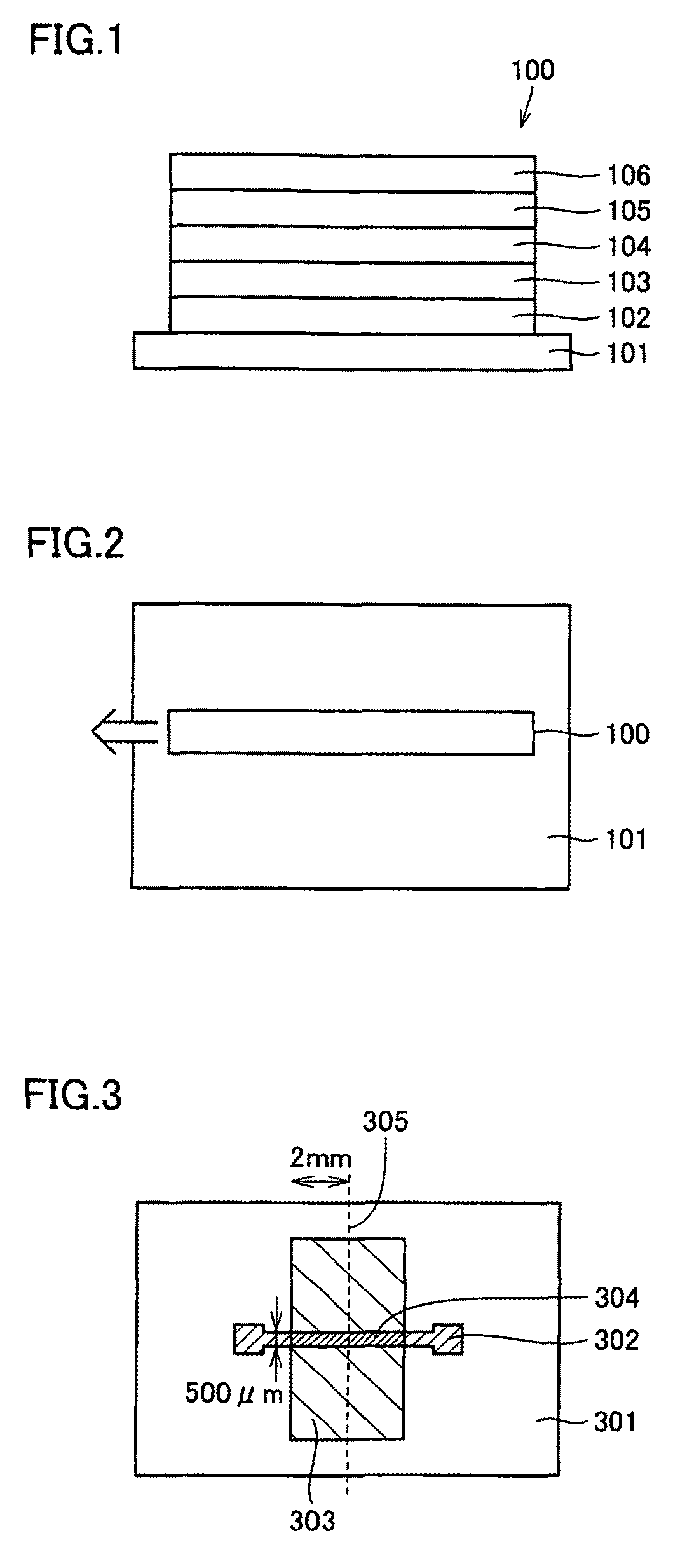
This will be described with reference to FIG. 3. FIG. 3 is a schematic top view showing a structure of an organic EL device manufactured in this example. First, a photoresist film having an aperture of 500 μm in width and 8000 μm in length was formed on a glass substrate 301 by photolithography and lift-off. Then, RF magnetron sputtering was executed to form an ITO layer of 30 nm in thickness over whole glass substrate 301 (ITO target: 10 mass % of SnO2 and 90 mass % of In2O3, flow rate: Ar 30 sccm, pressure: about 1×10⁻¹ Pa, PF power: 20 W). Then, the photoresist film was removed together with the ITO film formed thereon to provide a substrate having a patterned anode layer 302 (ITO layer). This substrate was cleaned with a detergent and an organic solvent, and was subjected to UV-ozone processing.

Then, a hole injection / transport layer, a light emitting layer and an electron injection / transport layer forming an organic layer were formed in this order by vacuum heating deposition ov...

examples 2 and 3

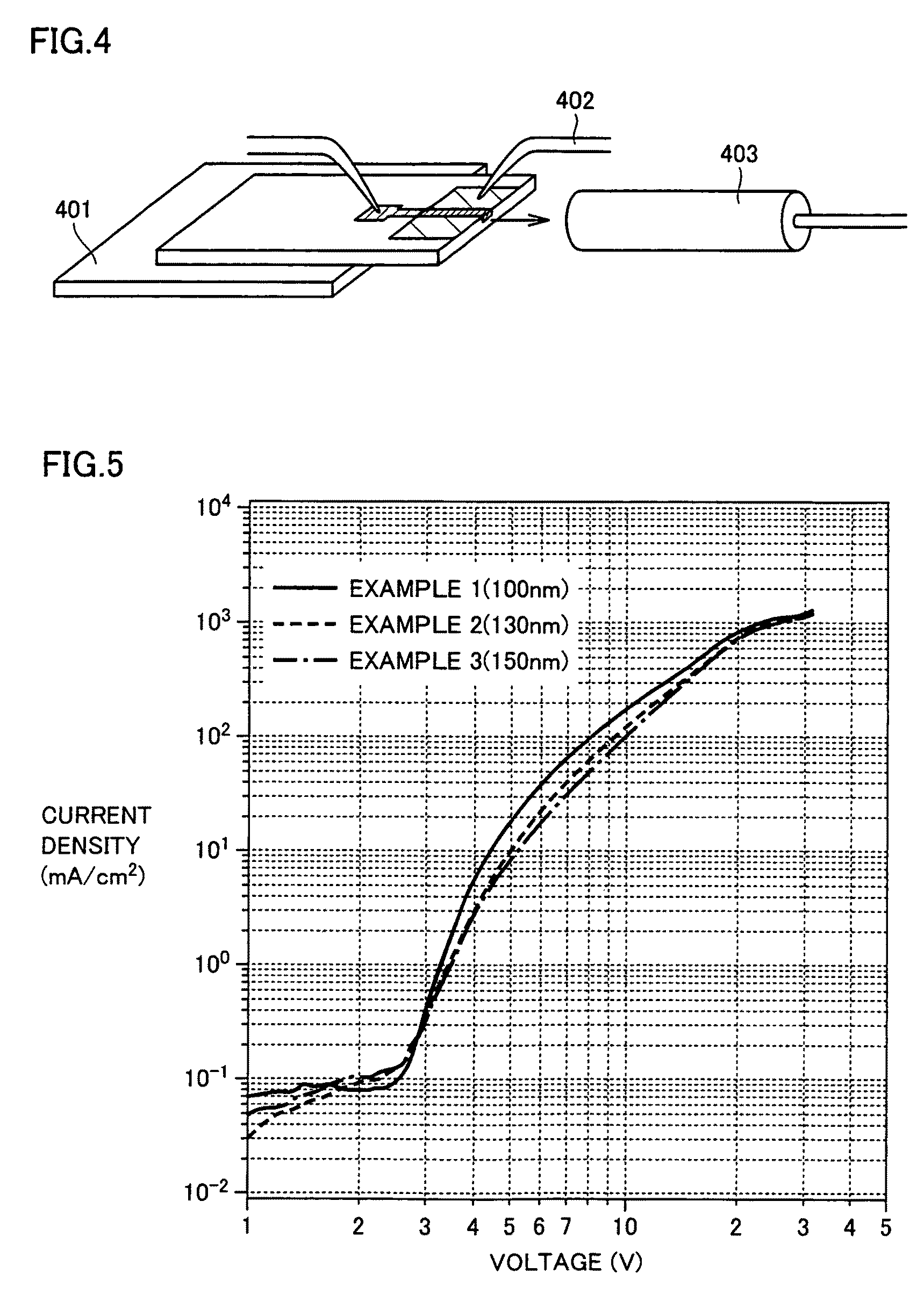
Organic EL devices were manufactured in the similar manner as the Example 1 except for that light emitting layers have thicknesses of 130 nm and 150 nm, respectively.

In the manufactured devices having the above film thicknesses, calculated values of the cut-off wavelengths of the optical waveguides were 456 nm, 479 nm and 499 nm with respect to the TE1 mode, respectively. As described later, these values are within the wavelength region of the full width at half maximum of the fluorescence spectrum of the BSB-Cz.


PUM


Abstract

An organic electroluminescence device, includes a substrate; an anode layer; an organic layer including at least one organic material having a fluorescence spectrum; and a cathode layer, wherein the organic electroluminescence device has a primary light outgoing direction that is parallel to a surface of the substrate, wherein the organic electroluminescence device has an optical waveguide that includes a core layer formed by the anode layer and the organic layer, and a clad layer formed by the substrate and the cathode layer, and wherein the optical waveguide has cutoff wavelengths in a transverse electric mode any one of which is within a wavelength range of a full width at half maximum of the fluorescence spectrum of any one of the organic materials included in the organic layer.

Description

BACKGROUND OF THE INVENTION1. Field of the InventionThe present invention relates to an organic electroluminescence device (which may also be referred to as an “organic EL device” hereinafter) and an organic laser diode, and particularly to an organic EL device and an organic laser diode that can emit light of an extremely narrow spectral width even with a lower current density.2. Description of the Background ArtAn organic semiconductor light emitting device such as an organic EL device has a simpler device structure than an inorganic semiconductor light emitting device, and can provide light of a shorter wavelength, e.g., from about 400 nm to about 550 nm so that it can have a larger capacity (higher recording density). Therefore, application to various fields has been expected, and search and development thereof have been actively conducted in recent years.Actualization of an organic laser diode has been expected as a next-generation technology following the organic EL device. It...

Claims


Application Information

Patent Timeline
Patent Type & Authority Patents(United States)
IPC IPC(8): H01J1/62
CPCH01S5/36H01L51/5262H01L51/52H01L51/5052H01L51/5088H01L2251/558H10K50/155H10K50/165H10K50/17H10K50/80H10K50/85H10K2102/351
Inventor YOKOYAMA, DAISUKENAKANOTANI, HAJIMEYAHIRO, MASAYUKIADACHI, CHIHAYAMORIWAKE, MASATOOHNISHI, DAISETOGUCHI, YOUSUKE
Owner KYUSHU UNIV
Why Eureka
Try Eureka